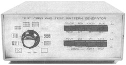
Electronic
Projects Online - Testcard Generator
Originally published
by Paul Stenning
in ETI, December 1991 and January 1992
Tom Payne has developed
a method of replacing the SAA1043 with a SAA1101, and kindly supplied
details. Link is in the list below.
Introduction
There have been several designs of test pattern
generators published in the past, invariably they produce the standard
cross-hatch pattern, possibly horizontal and vertical lines, and may-be
a grey-scale. Most current designs are based around the ZNA234E monochrome
test pattern generator IC.
 This
is adequate for monochrome (black and white) equipment, however for servicing
colour televisions and video recorders, something a little more comprehensive
is really required. The instrument featured here provides an impressive
range of patterns including a full colour Test-Card, colour bars, crosshatch,
grey-scale, focus grid, colour purity patterns and more - for considerably
less cost than a commercial unit of lower specification!
This
is adequate for monochrome (black and white) equipment, however for servicing
colour televisions and video recorders, something a little more comprehensive
is really required. The instrument featured here provides an impressive
range of patterns including a full colour Test-Card, colour bars, crosshatch,
grey-scale, focus grid, colour purity patterns and more - for considerably
less cost than a commercial unit of lower specification!
The unit also features a basic sine-wave audio
oscillator, set at 800Hz. The audio and video outputs are available from
the audio and video output sockets and, for more modern equipment, the
SCART socket. An RF modulator is provided for connection to the aerial
socket of UK standard Televisions and Video Recorders (readers in other
countries using the PAL standard may need to obtain a suitable type of
modulator locally). The audio and video signals to the modulator are individually
switchable to either the internally generated signals or to the external
audio and video input and SCART sockets.
A Scope Trigger Output socket is provided to
give reliable triggering on an oscilloscope when trying to view the video
signals, the output from this can be switched to either line or frame
sync.
Features and Specifications
Test Card: Full
colour Test-card featuring colour bars,
grey
scale (0%, 25%, 50%, 75% & 100%),
frequency
bars (0.5, 1.0, 1.25, 1.66, 2.5 & 5.0 MHz),
cross
hatch, low frequency blocks & needle pulse.
Other Patterns: Colour
bars 1 (black to white),
Colour
bars 2 (white to black),
Cross
hatch, Vertical lines,
Horizontal
lines, Dots, Focus grid,
Blank
raster, White raster.
Colour/Mono Switch: Removes chrominance
(colour information) from Video
signal,
thereby converting colour bars to grey scale,
and
removing herringbone patterns.
Red/Green/Blue Completely
remove information for that colour
Switches: from
video signal.
Internal Audio: 800
Hertz (nominal) Sine wave.
Video Out: 1V
Pk-Pk PAL Composite video from pattern generator,
BNC
socket.
Audio Out: 500mV
RMS, 800Hz Sine Wave, Phono socket.
Video In: 1V
Pk-Pk PAL Composite video, Input Impedance 75R or
500K
switchable, BNC Socket.
Audio In: 500mV
RMS into 10K, Phono socket, 30Hz to 15KHz +/-3dB.
SCART Socket: All
signal levels as above.
Pins
1 & 3, Audio out.
Pins
2 & 6, Audio in.
Pin
19, Video out.
Pin
20, Video in.
Pin
8, +12V via 4K7.
Pins
4,14,16,17,18 & 21, Ground.
Other
pins not connected.
RF (UHF) Output: UK
Channel 36 (591.5MHz) with 6MHz Sound Carrier.
Phono
socket.
Scope Trig Output: 5V Pk-Pk
@ 10K, switchable Line or Frame.
Power Input: 220-240V
AC 50Hz @ 6VA or 11 to 13V DC @ 120mA (see text).
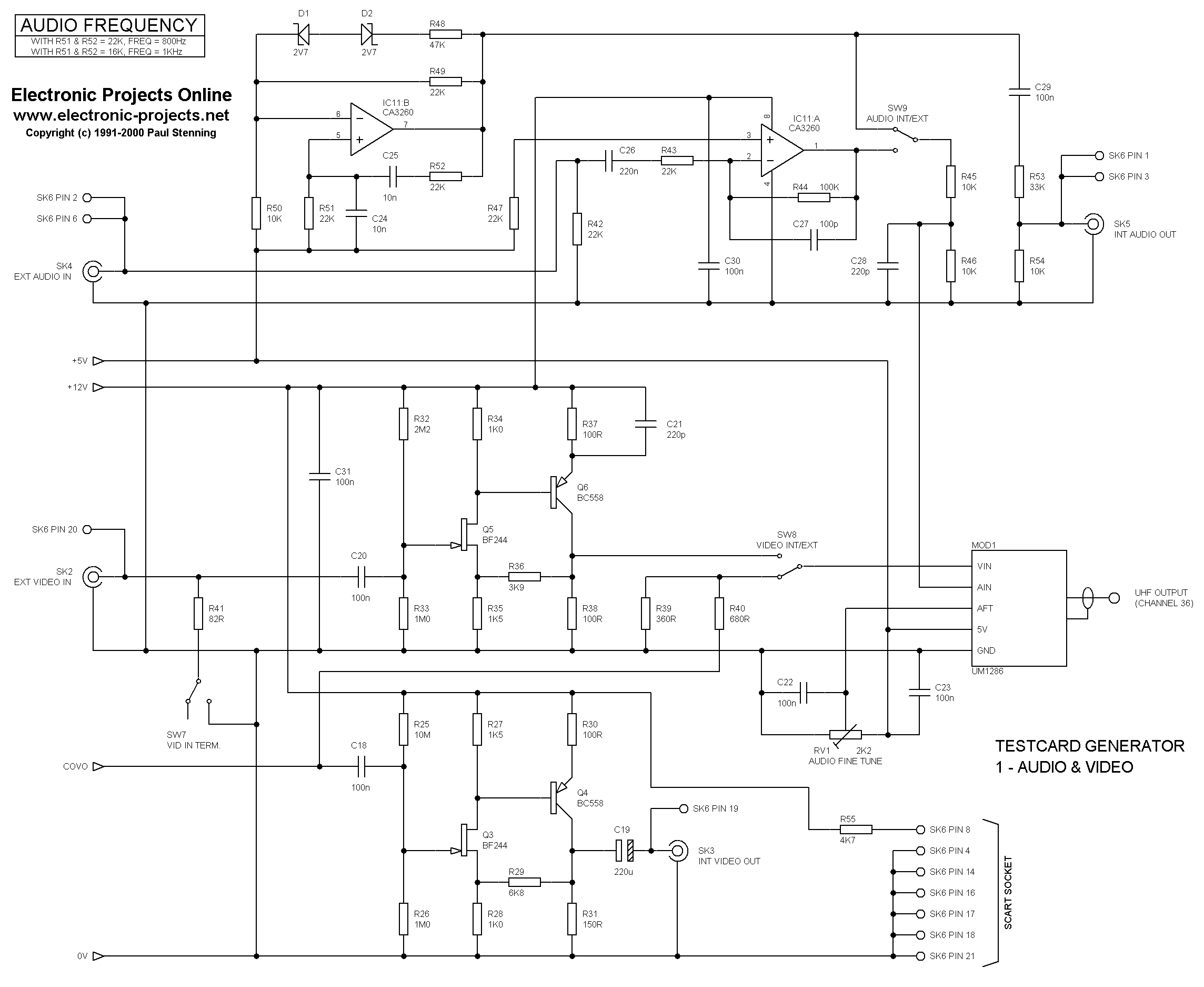
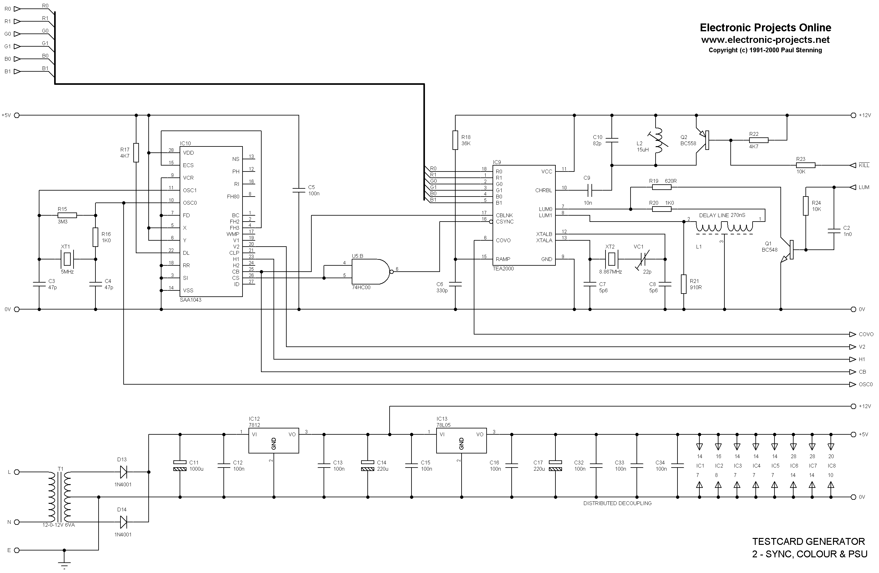
How it Works
Most of the difficult work is done by IC9 (TEA2000),
the PAL Colour Encoder IC, and surrounding circuitry. This IC produces
the luminance (brightness) and chrominance (colour) signals and combines
them to form the PAL standard composite video output. The IC requires
6 bit colour data, giving a total of 64 possible colours; it also requires
composite sync and blanking signals which are produced by IC10 (SAA1043),
a Universal Sync Generator IC. Various other signals are obtained from
IC10 for use as clock and timing signals for the remainder of the logic
circuitry. The H1 and V2 signals from this IC go to SW1, which selects
the signal to connect to SK1 (Scope Trig Socket) via R4. The colour data
required by IC9 is stored in EPROMs IC6 & IC7. IC6 contains the data
for the test card whilst IC7 contains the data for the other patterns.
As mentioned previously, IC9 is capable of
producing 64 colours, however for this application only 10 are required.
There are 2 data lines on IC9 for each of the 3 primary colours, labelled
R0 & R1 for red, G0 & G1 for green and B0 & B1 for blue. Taking
the red lines for example, if R0 only is high a fairly dark red (50% of
maximum brightness) is produced, if R1 only is high the colour is brighter
(75% of maximum brightness), if R0 and R1 are both high the colour is
maximum brightness (saturated, the same brightness as white), and if R0
and R1 are both low no red is produced. The same arrangement applies for
the green and blue data lines. By applying various codes to the data lines,
the primary colours can be mixed in various combinations to produce an
impressive range of colours.
The truth table below shows the codes required
for the ten colours used in this application:
Colour R0
R1 G0 G1 B0 B1
---------------------------------------
Black 0
0 0 0 0 0
Blue 0
0 0 0 0 1
Red 0
1 0 0 0 0
Green 0 0
0 1 0 0
Magenta 0 1
0 0 0 1
Cyan 0
0 0 1 0 1
Yellow 0 1
0 1 0 0
Dark Grey 1 0 1
0 1 0
Light Grey 0 1 0
1 0 1
White 1 1
1 1 1 1
From the above truth table it can be seen that
all the colours except black, white and grey are used at the 75% brightness
level, this level is chosen mainly because a good grey-scale is produced
if the colour bar pattern is selected and the chrominance (colour information)
is disabled. The logic levels on lines R0, G0 and B0 are always the same,
these 3 lines therefore share one data line (D0) from the EPROMs, leaving
more data lines available for other purposes. R1, G1 & B1 are connected
to data lines D1, D2 & D3 respectively.
Unfortunately the TEA2000 (IC9) will only produce
2 shades of grey, 50% and 75%, for the test card an additional grey at
25% is required. This is achieved using Q1 and R19 to reduce the luminance
signal level at the luminance delay line. This transistor is controlled
by data line D4, when the 25% grey is required, the 50% grey is selected
and D4 is taken high (a slight problem with this arrangement is that when
the test card pattern is selected, and all 3 colours are switched off,
a faint pattern will still be present, however since the instrument would
never be used in this manner, it was not considered important).
The address lines of the EPROMs, IC6 &
IC7 are controlled by two counter IC's, IC2 & IC3 (note that only
one EPROM, either IC6 or IC7, is selected at any one time, depending on
the position of SW2). The first counter, IC2 (74HC4040), is clocked by
a 5MHz clock signal taken from the crystal (XT1) of IC10 (via IC1:B);
the counter is reset at the end of each scan line by the composite blanking
signal (CB), also from IC10. This counter controls the EPROM address lines
A0 to A7. During the non-blanked period of a scanned line (when CB is
low) there are actually 258 clock pulses, so lines A0 to A7 count up from
0 to 256 (00h to FFh), then to 0 and 1 (00h and 01h) again. The fact that
the first two "pixels" in each line are repeated again at the end of the
line is of no consequence since this has been allowed for when planning
the pattern data.
A second counter chip, IC3 (74HC4024), is normally
clocked on each line by the composite blanking signal (via IC5:A), and
reset at the end of each frame by the V2 (Vertical Pulse 2) signal, also
from IC10. Six output lines from IC3 control the remaining six address
lines on IC6 (we will come to IC7 later), however since there are only
six address lines this gives a maximum count of only 64 lines. Since there
are about 280 visible lines per half frame (remember the 625 lines are
made up over 2 frames), some means of obtaining the 280 lines is required.
The obvious approach would have been to use larger EPROMs (more address
lines), however these could be difficult to obtain and get programmed,
and would make the unit more complex and expensive than planned. The Test-Card
pattern has many sections where one line is repeated several times over,
so the following arrangement was designed, where the same data in the
EPROM could be used for several lines if required. If data line D7 goes
high the rising edge resets another counter, IC4 (74HC4024), via C2 and
R2. Output line Q5 of this IC goes low which switches the CB signal off
of IC3 and on to IC4, via IC5:A and IC1:B. After 16 pulses on the CB line,
line Q5 goes high again, switching the CB signal back onto IC3. Therefore
if D7 is high during a picture line, that line is repeated 16 times. With
careful pattern programming the 64 sets of line data produced the required
full 280 line picture.
The above arrangement is fine for IC6, the
Test-Card EPROM, which only contains one frame, IC7 on the other hand
contains the data for 8 patterns. However these other patterns are made
up of only 8 picture lines repeated several times over to make up the
frame. Therefore only the lower 3 address lines from IC3 need to be connected
to counter IC7, the upper 3 address lines from IC7 are connected to positions
2 to 8 of SW2 (Pattern Select), via diodes D3 to D11, which act as an
8 into 3 line binary decoder, in conjunction with pull-up resistors R6
to R8. Switch position 1 selects IC6 and disables IC7, giving the Test-card
pattern.
The data line outputs of IC6 and IC7 are connected
to an 8 bit D-type latch, IC8 (74HC574). This latch is clocked by the
5MHz clock via IC1:C. The main purpose of this is to remove the effects
of the propagation delays of IC2 and IC6/IC7, which would otherwise give
rise to black vertical lines on the picture, particularly at points where
several address lines are supposed to change state simultaneously. IC8
is also used to produce the 5MHz part of the frequency grating on the
test-card. If line D6 is high the 5MHz clock signal is applied to the
OE (Output Enable) pin of IC8, due to IC5:C & IC5:D. When this clock
signal is high the outputs are disabled and are pulled low by resistors
R11 to R14, when the clock is low the outputs are enabled and high due
to D0 to D3 being high; thereby giving a 5MHz signal on all the colour
data lines. The outputs of IC8 are also disabled (due to IC5:C) when SW2
is in position 9, giving the Blank Raster pattern.
The colour data outputs of IC8 connect to IC9
via switches SW3 to SW5. These switches enable each of the primary colours
to be switched on or off independently.
If switch SW6 (Colour/Mono) is closed, Q2 is
turned on which removes the chrominance from the signal by effectively
shorting out the chrominance filter circuit (L2 & C10) of IC9.
The composite video output from IC9 (COVO),
is attenuated by R39 and R40, and fed to SW8 (the Int/Ext Video switch);
it is also buffered by a video amplifier comprising of Q3, Q4 and surrounding
circuitry, and fed to the Video Output socket (SK3), and pin 19 of the
SCART socket (SK6). The external video input from SK2 or pin 20 of SK6
is amplified by another similar video amplifier circuit, built around
Q5 & Q6. The input impedance of this amplifier is about 500K, but
can be reduced to about 75R by closing SW7. The output of this amplifier
is also fed to SW8. Either the internal or external video, as selected
by SW8, goes to the RF modulator MOD1.
The audio oscillator is built around IC11:B
and is a standard Wein Bridge circuit, with zener diodes used to control
the negative feedback. The output is connected to SW9; and also attenuated
to 500mV RMS (by R53 and R54), and fed to the Int Audio Out socket (SK5),
and pins 1 & 3 of the SCART socket (SK6). The frequency is set to
800Hz, but can be changed to 1KHz if required by reducing R51 and R52
to 16K.
The External Audio input is amplified by IC11:A.
The gain is arranged such that a 500mV input gives the same drive to the
modulator as the internal audio generator. The bandwidth is limited to
30Hz-15KHz by C26 and C27. The output also goes to SW9. IC11 is powered
from the 12 volt supply, with the 5 volt supply used as the mid-rail.
The outputs are about 8 volts peak-to-peak, centred at the 5 volt level.
SW9 selects either the internal or external audio, and R45 & R46 reduce
the level to about 4 volts peak to peak, centred at 2.5 volts, which is
the correct level for the RF modulator, MOD1. C28 removes the small amount
of 6MHz carrier signal that seems to come out of the modulator's audio
input, and would otherwise find its way onto the Audio Output socket.
RV1 is the 6MHz audio carrier fine tuning control.
The power supply uses a standard 12-0-12 volt
centre tapped mains transformer, with full-wave rectification, giving
about 17 volts DC across C11. This is regulated to 12 volts and 5 volts
using two standard 3-pin regulator IC's (IC12 and IC13).
If required T1 could be removed, IC12 linked
out, and the circuit powered from 12 volt (+/- 1 volt) batteries for portable
use. Current consumption at 12 volts is about 120mA, so a small rechargeable
sealed lead-acid battery would be a good choice. The maximum supply voltage
for IC9 is 13.2 volts, so ensure this is never exceeded (disconnect the
battery when recharging).
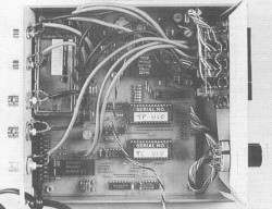
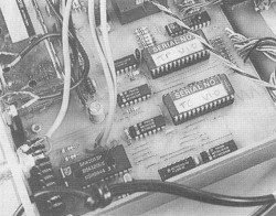
Construction
All the components except the switches, sockets
SK1 to SK5, mains transformer T1 and resistor R4 are mounted on the PCB.
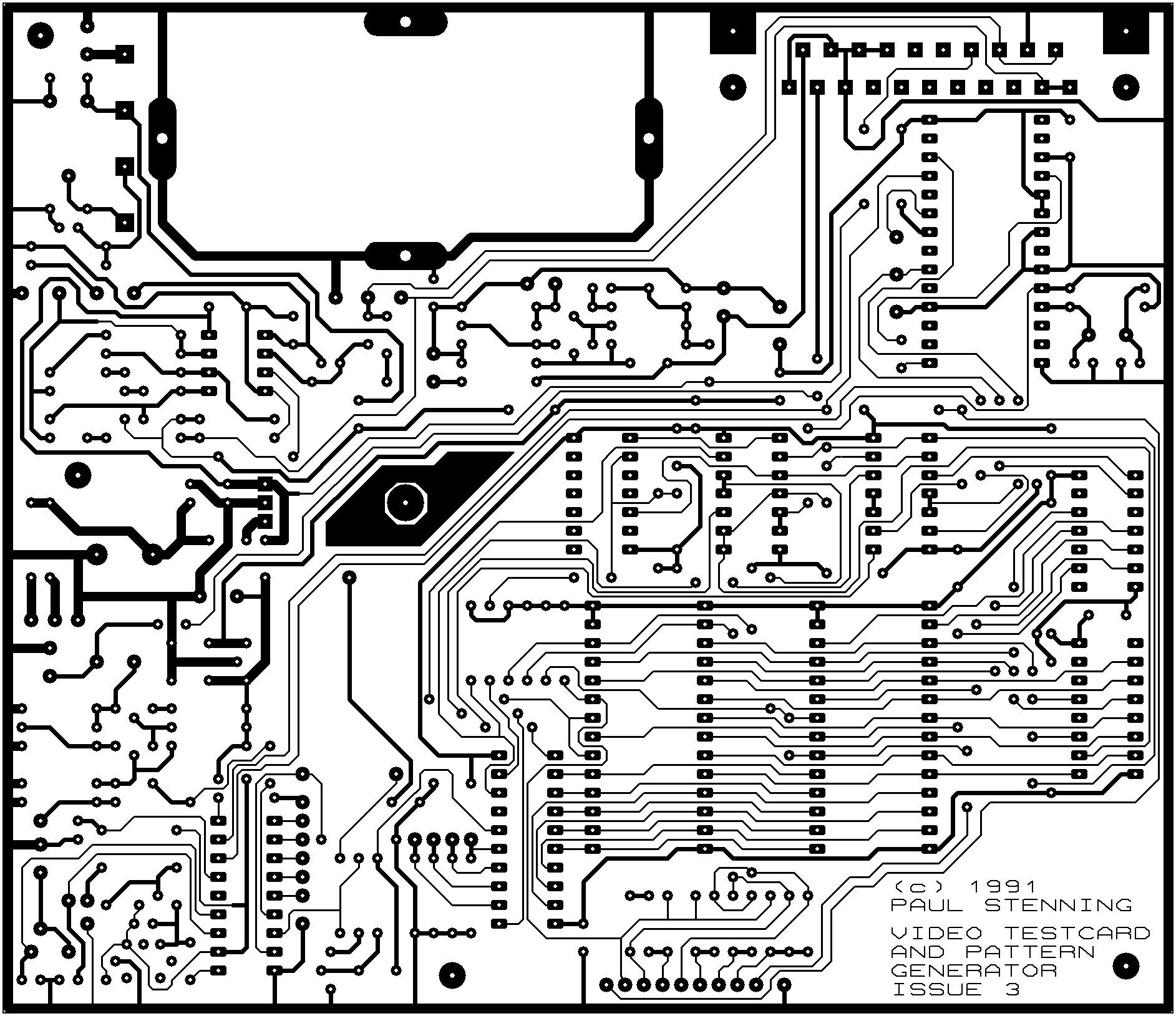
This is a single sided board, about 185 x 165 mm in size, and is available
from the ETI PCB service, order number ****, see page ***. There are 45
links and it is advisable to fit these first, using tinned copper wire,
about 24 SWG. The remaining components can then be fitted in the usual
size order. Note that there are tracks between many of the IC pins so
a fine tipped soldering iron and due care should be used. All the IC's
except IC12 and IC13 (the regulators) should be fitted in sockets, and
should not be inserted until the power supply voltages have been checked
- see Testing and Setting-up. Veropins may be used for the off-board connections
if desired. Take care particularly when fitting the inductors, crystals
and variable capacitor since they are easily damaged by rough handling
and excessive heat. When fitting the modulator, ensure it is well down,
then twist the mounting tags by about 45 degrees and solder. Do not connect
the wires from the modulator to the board until the power supply voltages
have been checked.
 The
prototype was housed in a plastic case approximately 170x70x190mm, however
this was a little tight for comfort. Since the instrument is mains powered,
a slightly larger earthed metal case would be more suitable. The PCB is
mounted at the rear of the case, with cut-outs in the rear panel for the
SCART socket and the UHF output socket on the modulator. The other sockets
are also mounted on the rear panel.
The
prototype was housed in a plastic case approximately 170x70x190mm, however
this was a little tight for comfort. Since the instrument is mains powered,
a slightly larger earthed metal case would be more suitable. The PCB is
mounted at the rear of the case, with cut-outs in the rear panel for the
SCART socket and the UHF output socket on the modulator. The other sockets
are also mounted on the rear panel.
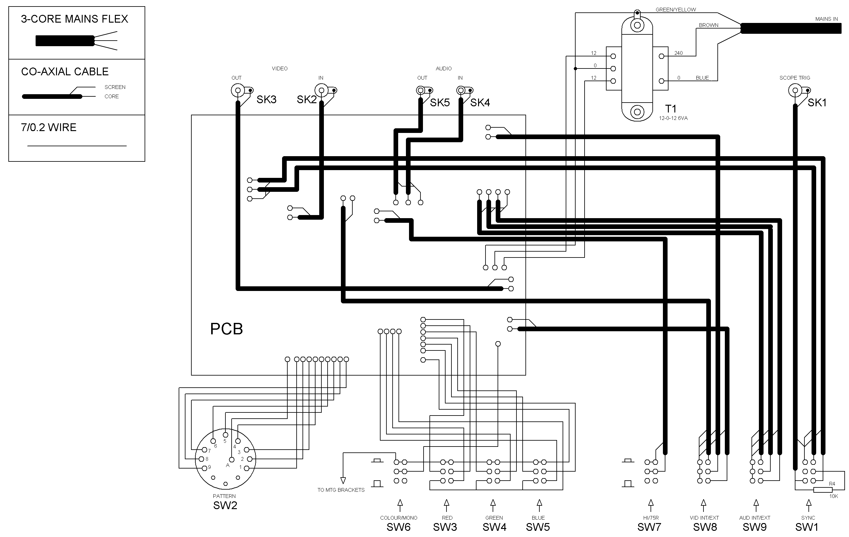
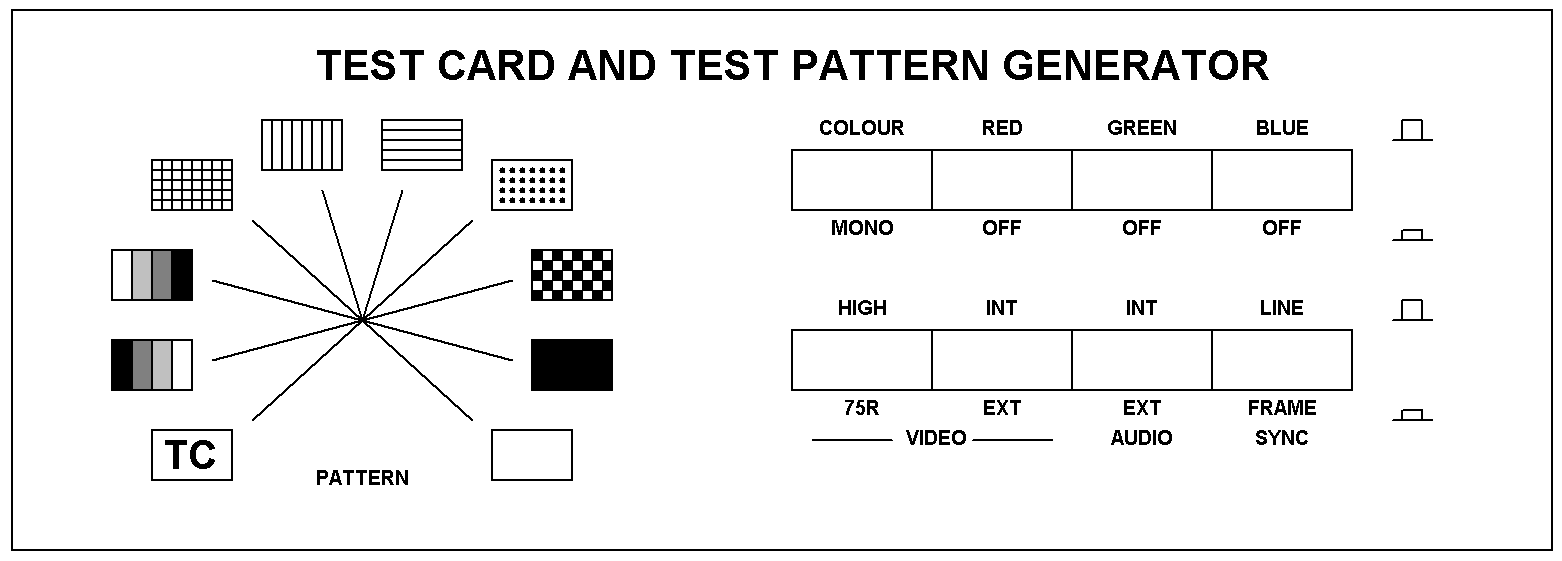
All the switches are mounted on the front panel,
a suitable legend is shown in fig **. Switch SW2 is a rotary type, 1 pole
12 way, with the stop set at position 10 (note that no connection is made
to pin 10, although position 10 is used). The other switches are the Japanese
type latching switches, and are mounted in two banks of four. The individual
switch latches are left in place and the interlocking mechanism is not
used.
The inter-wiring is shown in fig **, thin coax
cable is used for all signal wiring (proper 75R coax could be used for
the video but it is not too important with the lengths involved), and
standard hook-up wire for the remaining connections. The mains connections
should be insulated, and the flex secured in some manner. No mains on/off
switch or fuse were fitted on the prototype, however they could be fitted
if required. The mains plug should be fitted with a 3 amp fuse.
Testing and Setting-Up
Due to the cost of the modulator and some of
the IC's it is a good idea to check that the power supply voltages are
correct before fitting these parts. Make sure none of the IC's except
IC12 and IC13 are fitted, and that the modulator is disconnected. Give
the PCB a final visual check over, in particular watch for solder bridges
between IC pads and the tracks between them.
Connect the instrument to the mains, and switch
on. Set your test meter to 20 volts DC or thereabouts, and connect it's
negative lead to the case of the modulator. Check for 12 volts +/- 0.5
volts on pin 11 of IC9 socket, and 5 volts +/- 0.25 volts on pin 20 of
IC8 socket. If all is well switch off and wait a minute or so for the
power supply capacitors to discharge, then connect up the modulator and
fit the IC's. Most of the IC's are CMOS types but have protected inputs
so static damage is unlikely, however the usual handling precautions against
static discharge should still be taken.
Set SW2 to position 1 (full ACW); SW3, SW4
& SW5 on, SW6 off and SW8 & SW9 to Internal (all buttons out).
Connect the RF output socket on the modulator to your TV, cross your fingers
and switch on. You will probably need to tune your TV to channel 36, although
the channel you use for your video recorder should be somewhere near.
You should get an audio tone from the speaker and a test-card picture.
Don't worry at this stage if there is a buzz on the sound or no colour
in the picture.
To avoid damage to components and misleading
results, always use a proper trim-tool when making adjustments. Adjust
RV1 for minimum buzz (or to the middle of the area of no buzz) on the
sound. Adjust VC1 until the colour locks on, then set to the centre of
the range where you get colour. Finally adjust L2. If you have a 'scope
connect it to the Video Output socket and adjust for maximum amplitude
on the colour burst, otherwise adjust for brightest colour and minimum
"herringbone" pattern on the picture. All that remains now is to check
the various functions of the unit as detailed below. Once the unit has
been tested, the PCB can be fitted in the case, and the unit finished
off.
In Use
Firstly a word of warning. Anybody attempting
to repair or adjust Television Sets, whether using this instrument or
not, must be aware of the hazards involved. Many sections of TV circuitry
operate at dangerous voltages (in the range of 100V to 30KV), and in many
cases the internal chassis and metalwork is also at a dangerous (mains)
voltage. For maximum safety the set should always be powered via a mains
isolating transformer. If a transformer is not used, no test equipment
should be connected to the set, except to external sockets, and very great
care should be taken when making adjustments with the power on (the practice
of disconnecting the mains earth to all the test equipment is extremely
dangerous and should never even be considered). In any event always work
with one hand in your pocket when the set is on, even with an isolating
transformer the high voltages can be lethal. Care should also be taken
when working near the power supply of video recorders, although in this
case the rest of the circuit usually operates at more civilised voltages.
The use of an Earth Leakage Circuit Breaker on the mains feed to the bench
is also a sensible precaution.
In most cases the instrument would be connected
to the equipment under test via its aerial socket, since this enables
the whole signal path to be checked, also a fault in the equipment is
extremely unlikely to damage this instrument when connected this way.
Once the equipment has been proved to be basically sound, the instrument
could be connected by the video/audio or SCART connectors if required.
SW2 selects which basic pattern is produced,
as follows:
Position 1 Test
Card
2 Colour
Bars 1 (Black to White)
3 Colour
Bars 2 (White to Black)
4 Cross
Hatch
5 Vertical
White Lines
6 Horizontal
White Lines
7 White
Dots
8 Focus
Grid (Fine checker board pattern)
9 Blank
Raster (Sync & 0% video)
10 White
Raster (Sync & 100% video)
If SW6 (Colour/Mono) is pressed in, the colour
information will be removed from the picture, this will convert the Colour
Bars to Grey Scale, and remove the "herringbone" patterning on patterns
such as the Cross Hatch.
Pressing SW3/SW4/SW5 will remove the Red/Green/Blue
colour completely, this is the same effect as switching off that colour
gun inside the TV (with all three off there will be no picture). If this
is used in conjunction with the White Raster pattern, the sets colour
purity can be adjusted. It is also useful for removing the blue from the
Cross Hatch when starting to set up the convergence. (If SW3,4 & 5
are all switched off when SW2 is set to the test-card pattern, a faint
pattern will still be present - this should be ignored).
The features of the Test Card require further
comment. The overall size of the picture is slightly smaller than the
minimum size of a transmitted picture. The TV's picture height, width
and position controls should be adjusted such the whole test card is shown,
but with the tips of the corners very slightly hidden by the rounded corners
of the tube (you may find that some cheaper sets have the width adjusted
wider than this, this is because the width of the picture on these sets
varies with brightness). The overall brightness of the Test Card is about
that of an average picture. The background is dark grey (25%) with a white
Cross Hatch pattern, to enable the linearity to be checked.
 The
main area of interest on the Test Card is the centre section. Starting
at the top we have a black rectangle within white to check the LF response,
and a white needle pulse to check for reflections and instability. Next
we have a 250KHz, 100% to 0% square wave to test the transient response;
and below this are the eight colour bars. Next there is an six step frequency
grating with frequencies of 0.5, 1.0, 1.25, 1.66, 2.5 and 5.0 MHz. These
enable the frequency response of the video circuits to be checked, the
gratings up to 2.5 MHz should be clear and sharp, but many sets will have
trouble resolving the 5.0 MHz. Finally there is a five step grey scale
for adjusting contrast, with amplitudes of 0%, 25%, 50%, 75% and 100%.
The
main area of interest on the Test Card is the centre section. Starting
at the top we have a black rectangle within white to check the LF response,
and a white needle pulse to check for reflections and instability. Next
we have a 250KHz, 100% to 0% square wave to test the transient response;
and below this are the eight colour bars. Next there is an six step frequency
grating with frequencies of 0.5, 1.0, 1.25, 1.66, 2.5 and 5.0 MHz. These
enable the frequency response of the video circuits to be checked, the
gratings up to 2.5 MHz should be clear and sharp, but many sets will have
trouble resolving the 5.0 MHz. Finally there is a five step grey scale
for adjusting contrast, with amplitudes of 0%, 25%, 50%, 75% and 100%.
I will not go into further details of which
adjustments should be made with which pattern. I you have the service
manual for the equipment this will give suggestions, otherwise it's a
matter of experience and taste - if the set will give an acceptable picture
on all patterns there can't be much wrong! Some sets may have trouble
locking onto the output from this unit, in this case try switching off
the sets AFC and tuning manually. Remember that a test pattern is intended
to show the worst in a piece of equipment. At the end of the day the picture
should be acceptable to the viewer on a normal programme!
As its name suggests, the Scope Trig socket
can be used to externally trigger an oscilloscope when trying to view
the video signals inside the equipment. The output is 5 volts peak-to-peak
at 10K, and can be switched to either line or frame sync by SW1. Bear
in mind, though, that the outer of this socket is earthed inside the unit
so you may be earthing the TV's chassis via the 'scope leads.
When using the video and audio output sockets
it should be noted that the signals from these are always the internally
generated ones, regardless of the positions of the Int/Ext Video and Audio
switches; these switches only affect the output from the RF modulator.
This can be useful if, for example, a video recorder under test is connected
to the SCART socket, and the RF output connected to the workshop TV. The
signal from the generator can be compared to that from the video recorder
merely by operating the Int/Ext switches (no more fumbling with RF leads
behind the TV!). The unit can also be used to enable the composite video
and/or audio outputs from equipment such as video cameras and computers
(and certain satellite decoders!) to be fed to a normal TV via the aerial
socket.
Care should always be taken, particularly when
working on faulty equipment, to ensure that no excessive voltages are
applied to the unit, as this will almost certainly cause expensive damage.
Parts List
Resistors (all 1/4 Watt 5% or better)
R1,2,9,11,12,13,14,16,20,28,34 1K0
R3,4,5,6,7,8,10,23,24,45,46,50,54 10K
R15 3M3
R17,22,55 4K7
R18 36K
R19 620R
R21 910R
R25 10M
R26,33 1M0
R27,35 1K5
R29 6K8
R30,37,38 100R
R31 150R
R32 2M2
R36 3K9
R39 360R
R40 680R
R41 82R
R42,43,47,49,51,52 22K
R44 100K
R48 47K
R53 33K
RV1 2K2
Horizontal Preset
Capacitors
C1,2 1n0
0.2" pitch mylar
C3,4 47p
0.1" pitch ceramic
C5,12,13,15,16,18,20,22,23,29-34 100n 0.2" pitch
disc ceramic
C6 330p
0.1" pitch ceramic
C7,8 5p6
0.1" pitch ceramic
C9,24,25 10n
0.2" pitch mylar/ceramic
C10 82p
0.1" pitch ceramic
C11 1000u
25V radial elect
C14,17,19
220u 16V radial elect
C21,28
220p 0.1" pitch ceramic
C26 220n
0.2" pitch disc ceramic
C27 100p
0.1" pitch ceramic
VC1
22p Trimmer (Maplin WL70M)
Inductors
L1 Delay
Line 270nS (Maplin UH84F)
L2 15uH
Adjustable (Maplin UH86T)
Semiconductors
IC1 74HC02
IC2 74HC4040
IC3,4 74HC4024
IC5 74HC00
IC6,7 27C128-15
150nS EPROM
IC8 74HC574
IC9 TEA2000
IC10 SAA1043
IC11 CA3240
IC12 7812
IC13 78L05
Q1 BC548
Q2,4,6 BC558
Q3,5 BF244
D1,2 2V7
400mW Zener
D3-12 1N4148
D13,14 1N4001
Miscellaneous
MOD1 UM1286
UHF Modulator
SK1,2,3 Panel
BNC Socket
SK4,5 Panel
Phono Socket
SK6 R/A
PCB SCART Socket (Maplin FV89W)
SW1,3-9 DPDT
Latch Push Switch (Maplin FH87X)
SW2 1P/12W
Rotary Switch (Maplin FH42B)
T1
240 to 12-0-12 6VA
XT1 5.000000
MHz (Maplin UL51F)
XT2 8.867238
MHz (Maplin UH85G)
IC sockets (1 x 8 way, 4 x 14 way, 1
x 16 way, 1 x 18 way, 1 x 20 way and 3 x 28 way), Knob for SW2, Buttons
and brackets for SW1 & SW3-9 (Maplin FH61R & FH78K), PCB, Case
170x70x190mm (WxHxD) or larger, Coaxial cable, interconnection wire, tinned
copper wire (about 24 SWG), 3 core 3 Amp mains flex, 13A mains plug with
3A fuse, Phono plug to Co-ax aerial plug lead (Maplin FV90X), other leads
as required, grommet, nuts, screws & spacers.
Buylines
All Components except IC6, IC7 & IC8 could
be obtained from Maplin Electronic Supplies Ltd when the project was originally
written. The Maplin Order Codes for the more obscure components are given
in the parts list. The 74HC574 (IC6) & 27C128 (IC7/8) were listed
by RS/Electromail and several other suppliers.
The data for the EPROMs is provided in Intel-Hex
format - see link above. If you require a different format for your EPROM
programmer, you should download the software for the EPROM Programmer
Mk2 since this contains a utility to convert the data to many popular
formats.
Update (May 1992)
Update notes were published in the May 1992
edition of ETI. Many of these have now been incorporated into the main
text and diagrams, the remaining points are detailed below.
Modification
The wire from colour switch (SW6) to the PCB
should be co-ax to prevent stray pickup affecting chrominance level, a
hole is available on the PCB for the screen. The 0v link between SW6 and
SW3 should be removed and the switch mounting brackets connected to 0v
at SW5.
Buylines
It has come to the author's attention that
150nS 27C128 EPROM's are not too easy to come by. The prototype has since
been tested with 250nS EPROM's which work fine. It should be noted that
the EPROMs must be the CMOS 27C128 types, as normal 27128 devices consume
far too much power and will overload IC13 (the 78L05 regulator) causing
it to current limit.
Maplin have changed their range of 0.1" pitch
ceramic plate capacitors to ceramic disks with a 0.2" pitch, without changing
the order codes! These will fit the PCB if the leads are bent, or the
correct type can be obtained from RS/Electromail.