Test Patterns Available Vertical Bars
Horizontal Bars
Crosshatch
Dots
Fine Checkerboard
Coarse Checkerboard
White Screen
Blank Raster
8 Colour Bars (white to black)
8 Colour Bars (black to white)
White Level Switchable 75% or 100%
Colour Switching Primary colours individually switchable
Video System PAL (UK standard)
Composite Video Output Level 1V pk-pk into 75R
Audio Tone Frequency 1KHz (nominal) Sine Wave
Audio Output Level 1.2V pk-pk
UHF Output Channel Adjustable E30-E39, 6MHz sound subcarrier
Power Supply 230V AC, 50Hz, 6VA
PCB Sizes Main - 192mm x 145mm
Front - 97mm x 46mm
Overall Size 76mm x 203mm x 180mm (incl knobs etc)
Weight 850 grams (excluding leads)
Introduction
When servicing and repairing televisions and other items of video equipment, it can be helpful to have a stable and recognisable test signal. A colour bar pattern is often used for this, and indeed many television and video recorder service sheets use this type of signal as a reference.
 A variety of other
patterns are used for specific tests. For example, a crosshatch
is useful for checking picture linearity and convergence (colour gun alignment),
while a checkerboard pattern or dots are ideal for setting up the focus.
A variety of other
patterns are used for specific tests. For example, a crosshatch
is useful for checking picture linearity and convergence (colour gun alignment),
while a checkerboard pattern or dots are ideal for setting up the focus.The test pattern generator described here features these patterns as well as horizontal lines, vertical lines, dots, blank raster and white screen. The three primary colours are individually switchable. So for example the white screen can be switched to red, green or blue for checking colour purity.
There have been several designs for test pattern generators published in the past. Many of these are monochrome only and are often based on the ZNA234E IC. Published designs for colour units are often complicated, and therefore probably too expensive for occasional home use.
The aim of this design was to produce a straightforward reliable piece of equipment with no unnecessary frills and features. It should be possible to construct the unit for around seventy pounds including the case, which is much cheaper than commercial units having a similar specification. Setting up is straightforward and requires no test equipment.
This unit is an improved and updated version of a project by the same author, which was published in the March 1994 edition of "Electronics in Action" magazine. The original design was one of the most popular projects in the magazine, with over one hundred PCB's being sold. Since "Electronics in Action" is sadly no longer being published, and a couple of the components used in the original design are now obsolete, it was felt that now is the right time to publish this revised version.
A major improvement with this version is that construction has been simplified. The circuit is built on two PCB's, and requires no interwiring. The white level can now be switched to either 75% or 100%, so that the colour bar pattern can give a proper white reference level. The original Astec modulator is no longer available, so this unit uses an Alps modulator from Maplin. Since this modulator has sound capabilities, a 1KHz audio tone generator has been added. Other modifications have been carried out to improve performance and reliability.
The instrument is mains powered. A standard composite video output is available (1V pk-pk into 75R), as well as UHF modulated (UHF channel E36). An oscilloscope trigger output is also available, which is switchable to either line or frame sync, or to the audio oscillator.
Circuit Description
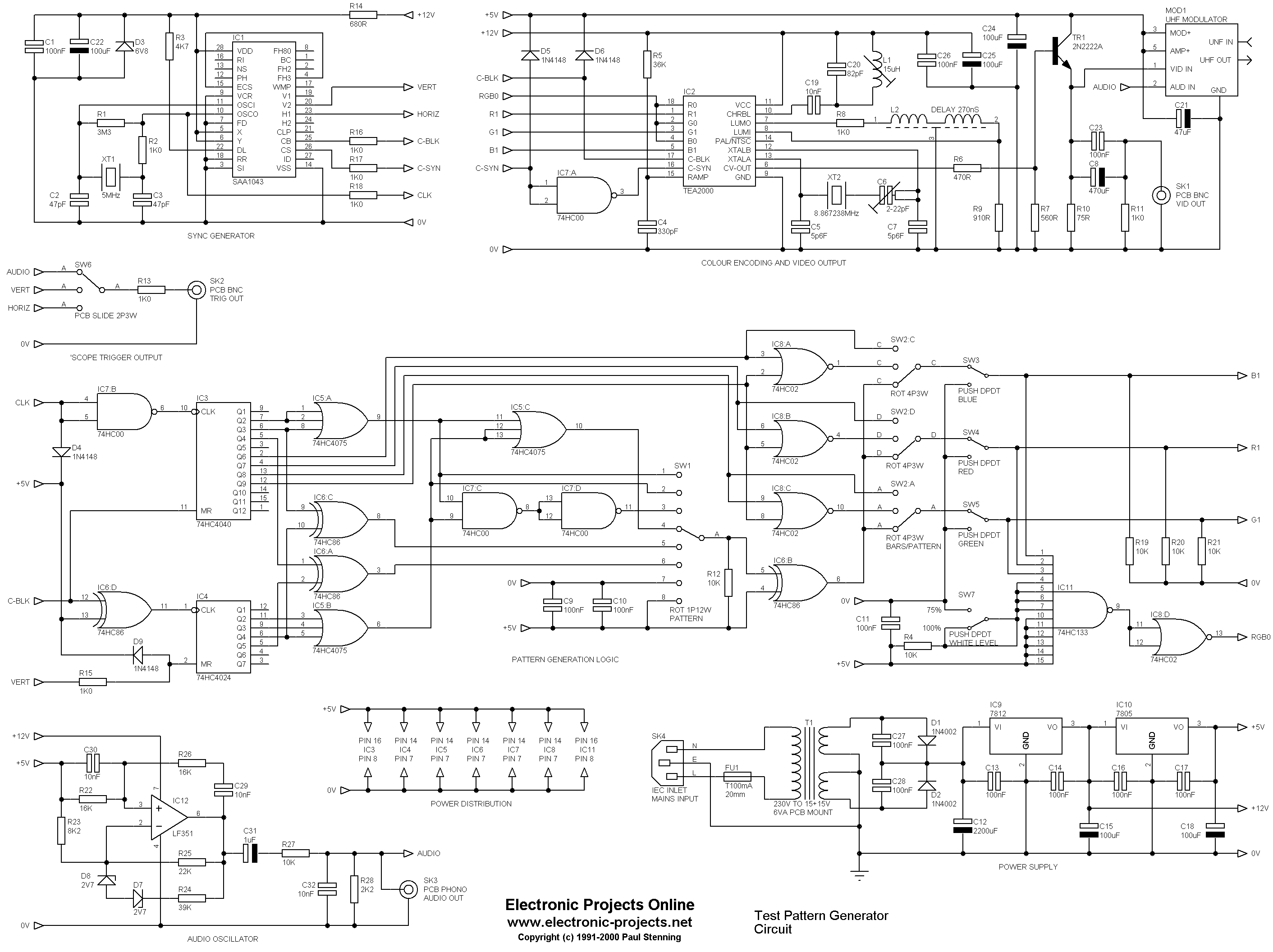
The circuit diagram is shown in figure 1. Most of the complicated stuff is handled by IC1 and IC2, which helps to simplify the remainder of the design. IC1 (SAA1043) is a universal sync generator, whose timing is controlled by XT1. In this design it is configured for the UK standard 625 line interlaced PAL, and four outputs are used.
IC1 requires a supply voltage between 5.7V and 7.5V. The SAA1043 has been operated with a 5V supply in several published designs (including some Maplin projects and the original version of this design). However experience has shown that a limited number of devices will not operate correctly at this voltage.
Since the current consumption of IC1 is very low (less than 1mA), it is powered by a 6V8 supply, which is derived from the 12V supply by a zener diode (D3) and resistor (R14). The output signals from IC1 are reduced to suitable levels for the 5V logic circuits by means of resistors (R15 to R19) and diodes (D4, 5, 6 and 9).
A 5MHz clock signal is derived from XT1. This controls the first binary counter (IC3, 74HCT4040), which is reset at the end of each line by the CB (composite blanking) signal. 258 clock pulses are counted by IC3 between each blanking pulse.
A second binary counter (IC4, 74HCT4024) counts the 312 or 313 CB pulses within a frame. This counter is reset by the VERT signal at the end of each frame. The fact that the counter has a capacity of only 128 is irrelevant in this case, since it merely wraps round.
The various patterns are derived from the outputs of these counters with some logic and switching. I will come back to this in a moment, once I've described the inputs required for IC2.
IC2 (TEA2000) is a colour encoder IC. To function it requires composite sync and composite blanking signals that are supplied by IC1. The colour inputs set the output colour. There are six such inputs, two for each primary colour. Taking the red inputs for example, if R0 is high a dark red is obtained, if R1 is high a brighter red is obtained, while if R0 and R1 are high a very bright red results. These equate to 50%, 75% and 100% brightness respectively. The device can produce 64 different colours although only nine are used in this design.
For the colour bars the R1, G1 and B1 lines are controlled in the appropriate sequence. For the black to white pattern, this is the binary output from three lines on IC3, while for the white to black pattern these three lines are inverted by three gates in IC8. Output Q9 of IC3 is connected to the three gates in IC8 to prevent a brief white bar appearing at the end of the white-to-black colour bars when the count on IC3 exceeds 255. Three sections of SW2 select either of these colour bar patterns, or connects the three lines to the monochrome pattern logic.
The R0, G0 and B0 inputs to IC2 are controlled by IC11 and IC8:D. If SW7 is set to the 100% position the output of IC8:D will go high when R1, B1 and G1 are all high. This gives a 100% white level. If SW7 is in the 75% position the output of IC8:D will remain low. Although a four input NAND gate would have been sufficient for IC11, the 74HC133 is the only 74HC series NAND (or AND) gate with more than three inputs in the Maplin catalogue.
With SW7 set to 100%, the white bar in the colour bar patterns will be brighter than the remaining colours (which are at 75%). This type of pattern is often specified in service manuals as the 100% white bar gives a true indication of the maximum video level, while the 75% colour levels are more representative of normal pictures. However if the colour bar signal is, for example, being recorded to fill the end of a video tape, setting SW7 to 75% may give a more pleasing appearance.
For the monochrome patterns, the R1, B1 and G1 lines are taken high or low together, giving white or black. IC11 and IC8:D operate as previously to give selectable white level. SW1 selects which pattern is displayed. The vertical bars are obtained from an OR gate on two outputs of IC3. The output of this OR gate is low when the three lines are low, this is inverted by the gate of IC6 after SW1. The horizontal lines are obtained by a similar arrangement on three outputs of IC4.
The crosshatch is obtained by an AND gate on the horizontal and vertical line signals, while the dot pattern is derived from an OR gate on these signals. The two checkerboard patterns are due to exclusive-OR gates on an output from each counter.
Two rotary switches (SW1 and SW2) were used for pattern selection, since the logic required to do the job with one switch would complicate the unit significantly, thereby adding to the cost. When SW2 is set to the "PAT" (pattern) position, the pattern selected by SW1 is displayed.
The three primary colours are individually switched by SW3, SW4 and SW5. The appropriate colour is on when the switch is in the out position. R19, 20 and 21 pull the appropriate lines low, to prevent flashing on the screen as the switches are operated (since the switches are break-before-make types). R12 serves a similar purpose with SW1.
L2 is a 270nS luminance delay line, which compensates for the delay caused by the chrominance filter formed by L1 and C20. L1 was found to be slightly prone to picking up noise from the digital circuits, so it has been positioned away from these on the PCB, and the board area beneath it is a ground plane. XT2 (8.867238MHz) is twice the PAL colour burst frequency, and is trimmed by a 2-22pF trimmer capacitor, C6.
TR1 buffers the output from pin 6 of IC2 for the composite video output (SK1) and the UHF modulator. The correct signal level is obtained by R6 and R7. C8 and C23 remove the DC offset from this signal. The large value of C8 is necessary to ensure there is no significant level shift during the frame blanking period, while C23 gives improved coupling at high frequencies.
The circuit around IC12 is a Wein bridge oscillator operating at 1KHz. Two zener diodes are used to control the amplitude of the waveform, since they are much cheaper than a bead thermistor. The zener diode arrangement only works with fixed frequency oscillators, such as this. The distortion is around 2%, which is adequate for this purpose. Note that the modulator itself has an audio distortion figure of 3%, so there is no point in providing it with a very low distortion signal. R27 and R28 reduce the audio signal to the correct level for the modulator. C32 removes the high frequency noise which emerges from the modulator audio input pin. The audio signal is also made available on SK3.
SK2 is intended for connecting to the trigger input of an oscilloscope, so that a stable trace may be obtained. SW6 selects the signal provided by this output, to either audio, video line or video frame.
The circuit requires 5V at about 180mA and 12V at about 70mA. Most of this current is consumed by the UHF modulator (160mA at 5V) and IC2 (60mA at 12V). The power is provided by a 6VA mains transformer and a pair of 78 series voltage regulators, which are mounted on small heatsinks. For safety the 0V rail is earthed.
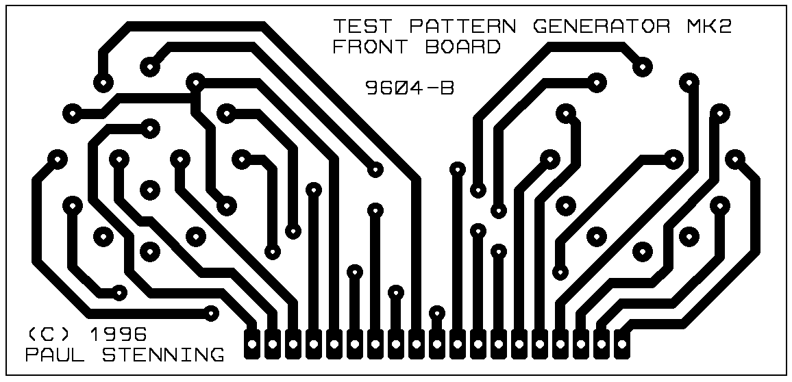
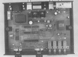
PCB Construction
 The circuit is
assembled on two single sided PCB's. The track layouts and component
overlays are shown in figures 2 and 3. Start with the wire links
(use 24 SWG tinned copper wire), and then fit the components in the usual
size order (starting with the smallest). Sockets may be used for
the IC's if desired.
The circuit is
assembled on two single sided PCB's. The track layouts and component
overlays are shown in figures 2 and 3. Start with the wire links
(use 24 SWG tinned copper wire), and then fit the components in the usual
size order (starting with the smallest). Sockets may be used for
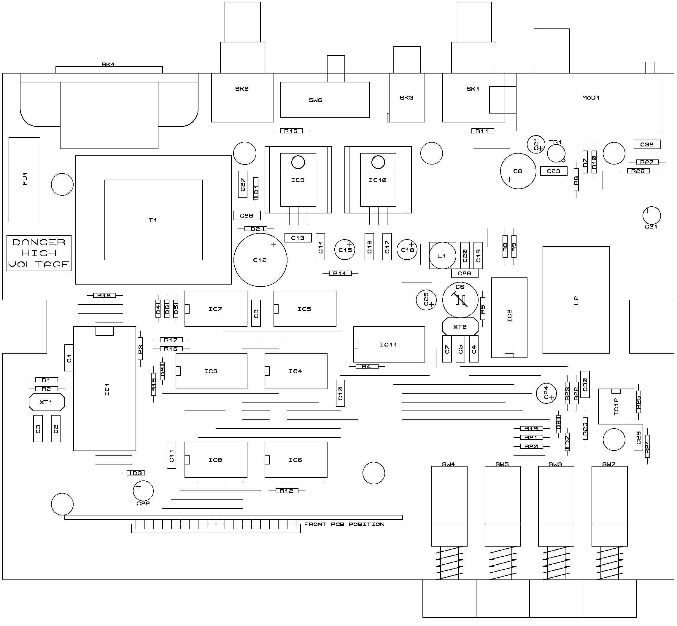
the IC's if desired.On the main board, switches SW3, 4, 5 and 7 should be assembled onto a four position latch bracket before being fitted to the PCB. The interlocking plate must be removed, and the individual switch latches retained. The knobs should also be fitted at this stage to avoid stressing the PCB later.
The voltage regulators (IC9 and IC10) must be fixed to small heatsinks and the PCB using M3 screws, nuts and washers. Although no electrical insulation is necessary, an insulator between the device and heatsink will improve the thermal coupling.
SK1 must be fitted before the modulator, because of the (unused) phono socket on the side of the latter. SK4 (IEC mains inlet) should be fixed to the PCB with M3 hardware prior to soldering. The transformer should be fitted last, because of its size and weight.
Before fitting SW1 and SW2 to the front PCB, the loops must be cut off the end of the tags. When doing so, be sure to leave the remaining tags as long as possible. SW2 should be positioned with the front panel locating tab towards the upper right corner as shown. The locating tabs are not used, and should be cut close to the body of the switches.
The two PCB's are linked using a 19 way length of right angle SIL header strip. This will need to be cut from a longer piece. The angled end of the pins must be fitted into the front PCB, so that the straight ends can then be fitted into the main PCB.
Case Assembly
The PCB's were designed to fit into the specified case. In the base of the case there are two flat tags towards the back which must be removed.
There are also a number of PCB fixing posts, of which only seven are used. The remaining posts must be shortened so that they do not foul on the underside of the PCB. This may be easily achieved using a sharp 8mm drill bit in a hand operated or SLOW electric drill (such as a rechargeable battery drill). Locate the tip of the drill bit in the hole at the top, and cut away each post until it is about half the original height.
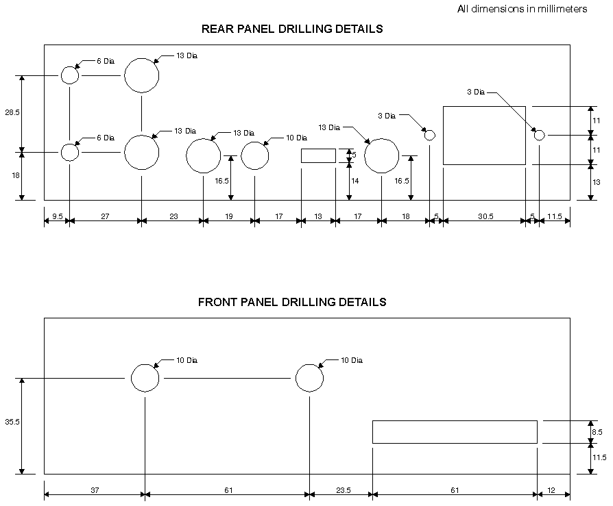
Drilling details for the front and rear panels are shown in figure 4. The rectangular holes may be cut by drilling holes in two opposite corners and then cutting out the remainder using a fret saw. This can then be finished with a small file.
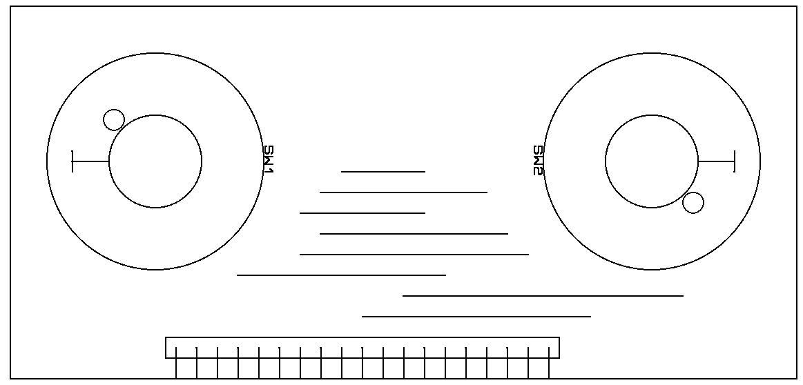
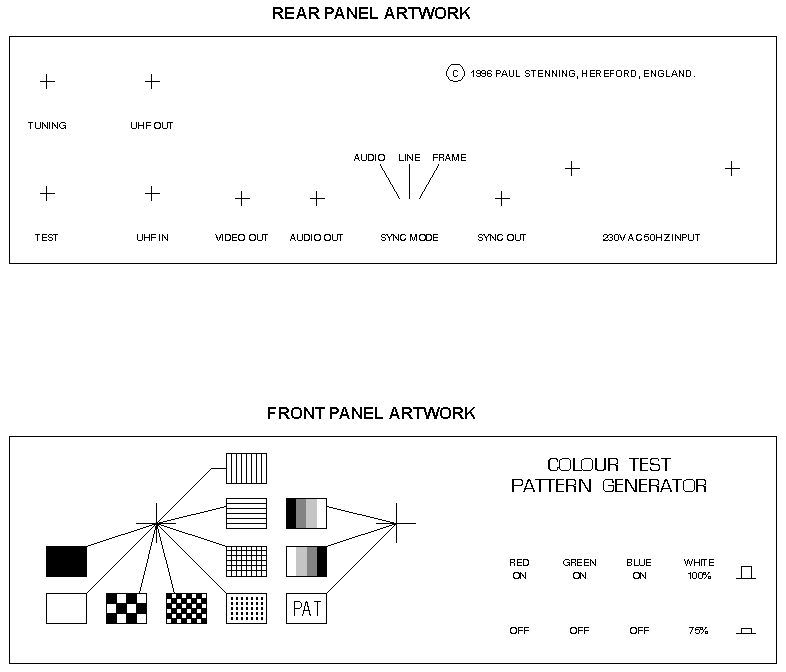
Suitable overlays for the front and rear panels are shown in figure 5. These may be photocopied onto a white A4 self-adhesive label and fixed to the appropriate panels. For durability they should then be covered with clear self-adhesive vinyl. The label and vinyl can then be trimmed around the holes using a sharp craft knife or scalpel. You may need to chamfer the inside edges of these panels slightly to allow them to fit into the case, because of the extra thickness on the outside.
Set the end stop of SW1 to eight positions, and SW2 to three positions, and then fit the front panel to the switches. The shakeproof washers supplied with the switches should be positioned between the switches and the panel. Cut the shafts down to about 8mm, then fit the knobs.
The rear panel should be fixed to SK4 using M3 hardware. The supplied nuts should be used to fix the panel onto SK1 and SK2 (discard the shakeproof washers).
The whole assembly should then be slotted into the base of the case. Depending on the accuracy of your drilling you may need to ease the mounting holes in the PCB slightly, so that they coincide with the posts in the case. The PCB is held in place using seven 6.35mm long No 4 self tapping screws. Do not overtighten otherwise the screws will strip the threads they have cut in the posts.
Testing and Setting Up
Providing the unit has been carefully constructed there is no reason why it should not work first time. Connect the unit to the mains using an IEC mains lead. If a test meter is available, check the +12V and +5V rails are correct on the appropriate pins of the voltage regulators.
Take care as there are mains voltages on the PCB. These are limited to the area around T1, FU1 and SK4, and are fairly inaccessible from above providing the cover has been fitted to the fuse holder - but due care must still be taken.
 Set
the small slide switch on the back of the modulator to the upper position.
Connect the UHF output to a television and tune in to UHF channel E36
(often used for video recorders and video games). You should be
able to tune in two white vertical bars (this pattern is generated within
the modulator). An audio tone should also be heard.
Set
the small slide switch on the back of the modulator to the upper position.
Connect the UHF output to a television and tune in to UHF channel E36
(often used for video recorders and video games). You should be
able to tune in two white vertical bars (this pattern is generated within
the modulator). An audio tone should also be heard.Set the switch on the modulator to the lower position. Ensure the four front panel push switches are out. Set SW2 fully clockwise and a set of colour (or monochrome) bars should appear. You may need to adjust the tuning on the television slightly.
Adjust C6 with a suitable trim-tool until the colour locks on. Adjust it back and forth to find the range of adjustment that gives a colour picture, then set it to the centre of this range.
Now adjust L1 for the clearest colours and a well defined edge where the colours change. This will probably be about a third of a turn up from the bottom. If an oscilloscope is available this can be connected to the video output and L1 adjusted to peak the amplitude of the colour information on the signal.
If SW2 is turned to the centre position, the direction of the colour bar pattern should reverse. Operate SW7 (White), and the brightness of the white bar should reduce.
If SW2 is now set fully anti-clockwise, the pattern displayed is controlled by SW1. Check SW1 works as expected, then set it to the white screen position and check SW3, SW4 and SW5.
If the unit is left on for a while, the voltage regulators (IC9 and IC10), the TEA2000 (IC2) and the mains transformer (T1) will become warm. You may also notice a faint smell of varnish from the transformer the first couple of times it warms up. This is normal, and should not cause concern.
Finally fit the top cover of the case, with the two plastic tabs to the rear.
In Use
The UHF modulator has a pass-through facility, similar to that on video recorders. The unit may therefore be connected between an aerial and the equipment being tested, so that the normal channels may be obtained without changing connections. Due to the digital nature of the unit and the signals produced, it may cause some interference on the normal channels unless the signal from the aerial is fairly strong. If this occurs you could try using an aerial amplifier between the aerial and the unit, otherwise you will need to use the unit separately.
The modulator UHF output is tuned to channel E36 when supplied. An adjustment screw on the back allows this to be adjusted between channels E30 and E39. This adjustment may be necessary if you are using the unit in conjunction with a video recorder or if you live in an area where Channel 5 is (or will be) broadcasting on channel E35 or E37.
The unit should be disconnected from the mains when not in use.
One final important comment - if you are working inside a television set or other piece of equipment with the power on, please be very careful.
Acknowledgements
The author would especially like to thank the former editor of "Electronics in Action" magazine, for granting permission to publish this design. He would also like to thank Maplin/MPS for supplying the components used to construct the prototype. The Maplin codes for the more critical components are given in the parts list).
Parts
Resistors (All 1% 0.6W Metal Film)
1 R1 3M3
8 R2,R8,R11,R13,R15,R16,R17,R18 1K0
1 R3 4K7
6 R4,R12,R19,R20,R21,R27 10K
1 R5 36K
1 R6 470R
1 R7 560R
1 R9 910R
1 R10 75R
1 R14 680R
2 R22,R26 16K
1 R23 8K2
1 R24 39K
1 R25 22K
1 R28 2K2
Capacitors
12 C1,C9,C10,C11,C13,C14,
C16,C17,C23,C26,C27,C28 100nF
2 C2,C3 47pF
1 C4 330pF
2 C5,C7 5p6F
1 C6 2-22pF
1 C8 470uF 16V
1 C12 2200uF 25V
5 C15,C18,C22,C24,C25 100uF 16V
4 C19,C29,C30,C32 10nF
1 C20 82pF
1 C21 47uF 16V
1 C31 1uF 63V
Inductors
1 L1 15uH Adjustable (Maplin UH86T)
1 L2 270nS Delay Line (Maplin UH84F)
Semiconductors
1 IC1 SAA1043 (Maplin UK85G)
1 IC2 TEA2000 (Maplin UH66W)
1 IC3 74HC4040
1 IC4 74HC4024
1 IC5 74HC4075
1 IC6 74HC86
1 IC7 74HC00
1 IC8 74HC02
1 IC9 7812
1 IC10 7805
1 IC11 74HC133
1 IC12 LF351
1 TR1 2N2222A
2 D1,D2 1N4002
1 D3 6V8 500mW
4 D4,D5,D6,D9 1N4148
2 D7,D8 2V7 500mW
Switches
1 SW1 1P12W Rotary (Maplin FF73Q)
1 SW2 4P3W Rotary (Maplin FF76H)
4 SW3,SW4,SW5,SW7 DPDT PCB Push (Maplin FH67X)
1 SW6 2P3W PCB Slide (Maplin FV02C)
Sockets
2 SK1,SK2 PCB BNC (Maplin KE15R)
1 SK3 PCB Phono (Maplin HF99H)
1 SK4 PCB IEC Inlet (Maplin FE15R)
Miscellaneous
1 FU1 20mm T100mA
1 FU1 20mm PCB Fuseholder (Maplin DA61R)
1 FU1 20mm Fuseholder Cover (Maplin DA62S)
1 MOD1 Alps MDLK6B UHF Modulator (Maplin WC20W)
1 T1 230V to 15+15V 6VA PCB (Maplin YJ55K)
1 XT1 5MHz
1 XT2 8.867238MHz
1 Case (Maplin BZ76H)
1 RF Flylead
1 Mains Lead
1 SIL R/A Header Strip
1 4 Way Latchbracket (Maplin FH78K)
4 Push Switch Knob (Maplin FH61R)
2 Knob (Maplin RW90X)
2 Heatsink (Maplin FL58N)
2 Insulator TO220 (Maplin QY45Y)
1 pkt 6.35mm No4 self tap scrw
1 pkt M3 x 10mm Pan head scrw
1 pkt M3 nut
1 pkt M3 washer
1 Main PCB
1 Front PCB