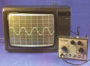 The Tele-Scope presented
here allows a normal television (black and white or colour) to be used as an
oscilloscope display. No modification is required to the television, connection
being made via the aerial (or video input) socket.
The Tele-Scope presented
here allows a normal television (black and white or colour) to be used as an
oscilloscope display. No modification is required to the television, connection
being made via the aerial (or video input) socket.The unit is reasonably low cost, and uses readily available components. Setting up is straightforward and can be carried out with no test equipment.
The Tele-Scope may be useful in education and other applications where a number of people need to view the display. The composite video output could also provide a useful way of incorporating waveform displays into training videos etc.
Advantages over a conventional oscilloscope include a display hold facility, and the absence of flicker on slower timebase settings.
Limitations
The unit is not a full oscilloscope and was designed to be made at reasonable cost. Consequently there are some limitations, and it is only fair that you are made aware of these before starting construction.
The most significant limitation is the input bandwidth (frequency range). The maximum frequency signal that the unit can display is 20KHz. This is due primarily to the A-D convertor used, faster 8 bit convertors are available but are considerably more expensive than the device used. Although this means the unit cannot be used with microprocessors, it is still useful for audio work, and digital projects which operate at lower frequencies.
The timebase settings are not convenient figures, due to the use of a divider on the main system clock (see 'How it Works'). However the time per division figures are given and the period or frequency of any waveform can easily be established (although a calculator may be required).
The input is not protected against excessive input voltages, since adding protection caused more problems than it solved. The Input Range attenuator will give some protection on all but the 10mV range. Fortunately the input amplifier IC is an extremely low cost device, and can readily be replaced if the worst happens!
Since the trace is made up of 256 dots it will not necessarily appear as a continuous line (see screen photo), however the shape of the trace will normally be apparent if a suitable timebase setting is chosen.
There is no external triggering facility.
If the signal is too large to display it will clip at the top and/or bottom of the display.
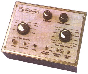
Features and Specifications
Input Voltage Range: 10mV/div to 30V/div in 8 steps
Input Coupling: AC or DC
Input Impedance: 1M nominal
Input Bandwidth (DC): DC to 20KHz
(AC): 2Hz to 20KHz
Trace vertical position: Adjustment with zero button
Timebase Range: 32uS/div to 66mS/div in 12 steps
Triggering Level: Adjustable, switchable to positive or negative going edge
Triggering modes: Automatic, Free Running, Display Hold
Graticle: 8 x 8 rectangles
Probe adjustment output: 1V pk-pk nominal at approx 1KHz
Video output: PAL Composite Video, approx 0.8V pk-pk into 75R
RF Output: UK Channel 36
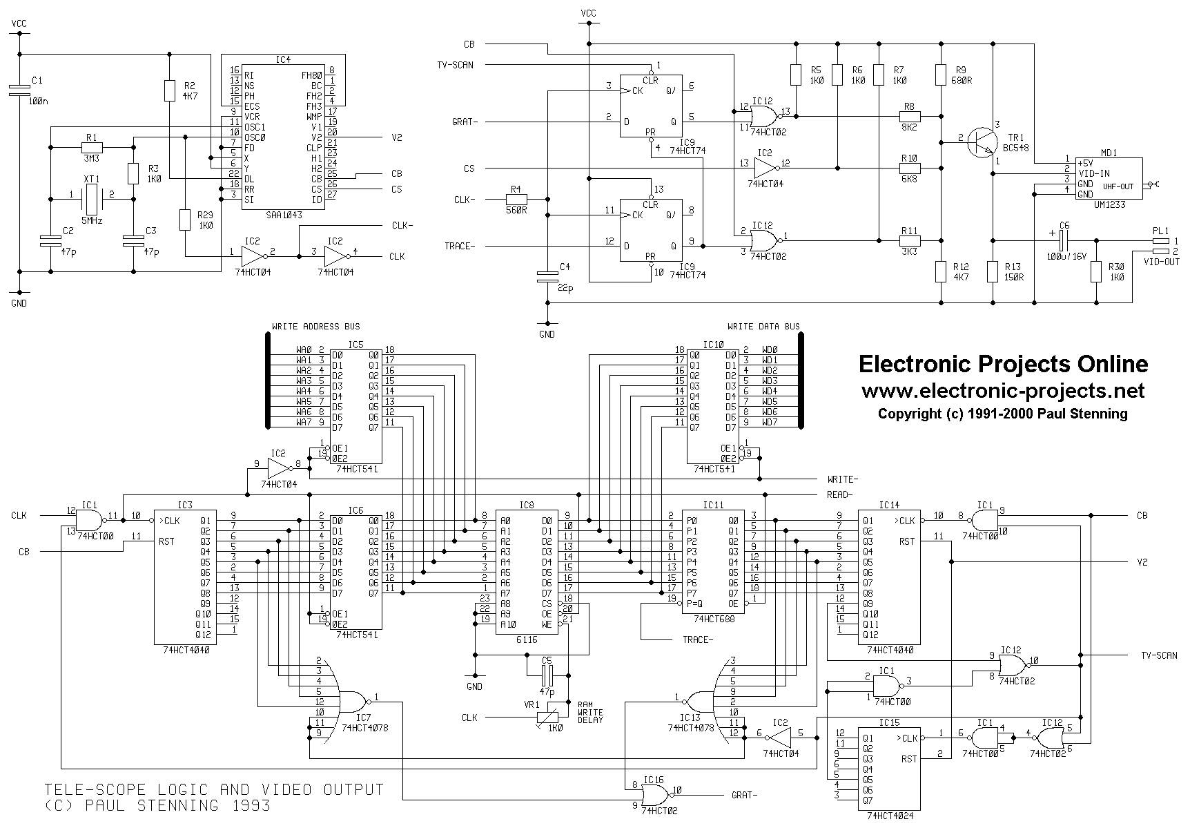
How it Works - Main PCB
The main circuit diagram is shown in fig ??, whilst the input circuit is shown in fig ??.
In this description, any signal name which is followed by a minus sign (eg READ-) is active low.
The heart of the circuit is IC8, a 2K 6116 RAM chip. One section of the circuit writes data from the A-D convertor into RAM, whilst another reads the RAM and displays the trace on the screen. These two processes run asynchronously, conflict being avoided by the use of tri-state buffers controlled by the READ- and WRITE- lines. This will all be explained in detail as we continue!
Only 256 RAM locations are used, the remaining address lines are tied low. A 2K IC was used because it was the cheapest device available, that was fast enough for this application. Each memory location contains a value between 0 and 255, which comes from the A-D. A value of 0 will give a dot in the appropriate position on the top active line of the display, whilst a value of 255 equates to the bottom line. The A-D gives a value of 0 for zero input and 255 for maximum input. This is the opposite of what is required and is resolved by an inverting stage in the input amplifier.
The timing of the whole circuit is controlled by IC4, a universal sync generator, which in this case in configured to operate in 624 line video game mode. This results in frames of 312 lines, and gives less flicker than standard 625 line interlaced mode, whilst rataining compatibility with 625 line PAL equipment. The circuit clock is derived from the crystal oscillator of this IC, via two gates of IC2.
Memory Read
The CB (Composite Blanking) line from IC2 is high during the frame sync period, and pulses high during the line sync period. Counters IC14 and IC15 are reset by the V2 signal, which pulses high during the frame sync. Initially pin 5 of IC15 is low so the CB pulses are fed to IC15. After 16 such pulses IC15 pin 5 goes high, switching subsequent CB pulses to IC14. The effect of this is to give 16 blank lines at the top of the screen before the display starts.
The next 256 CB pulses drive counter IC14, and these are the 256 active lines of the display. On the 256th pulse pin 12 of IC14 goes high, diverting the CB pulses back to IC15 for the remainder of the frame.
During the 256 active lines, the TV-SCAN line is high and the CLK signal is fed to counter IC3. This IC counts to 255 during each line, and is reset at the end of the line by the CB signal.
Hence we have two counters, one counting the active lines (0 to 255), and the other counting from 0 to 255 along each line. The graticle is generated by NOR gates on the Q1 to Q5 outputs of these two counters, resulting in a GRAT- signal.
The clock pulses to IC3 are also used as the READ- signal, and an inverted form of this is the WRITE- signal.
When READ- is low, the outputs of IC3 are coupled to the RAM (IC8) address lines via tri-state driver IC6. The READ- line also drives the RAM Output Enable (OE-) line, and the contents of the memory location addressed is output on the data lines. IC11 is a logic comparator, the output of which goes low if the data on P0 to P7 is the same as that on Q0 to Q7. This compares the output of counter IC14 with the data from the RAM, if the two are the same then a trace dot will appear on the screen (TRACE- signal).
The GRAT- and TRACE- signals are latched into two D-type flip-flops (IC9), which extend the pulses over the write period. The timing of the TRACE- signal is fairly critical (the pulse is short due to propogation delays), hence the time delay circuit on the clock inputs of the D-types. The signals from the D-types are combined with CB and CS (Composite Sync) through logic gates and resistors to form the composite video signal, which is buffered by TR1 before driving the modulator (MOD1) and the video output socket.
Memory Write
The timebase range is selected by choosing a division of the clock frequency, the division being carried out by IC17 (which divides by 5) and IC18. This is then fed to IC21 via the sync circuit (discussed shortly), the outputs of which drive the RAM address lines via IC5 when WRITE- is low. At the same time the output of the A-D drives the data lines of the RAM via IC10.
The timing of the Write Enable (WE-) pulses to the RAM are fairly critical, and appear to vary slightly with different makes of IC (we are running this device at the limit of its speed specification). For this reason a variable time delay is incorporated, which can be adjusted for best results with the device used.
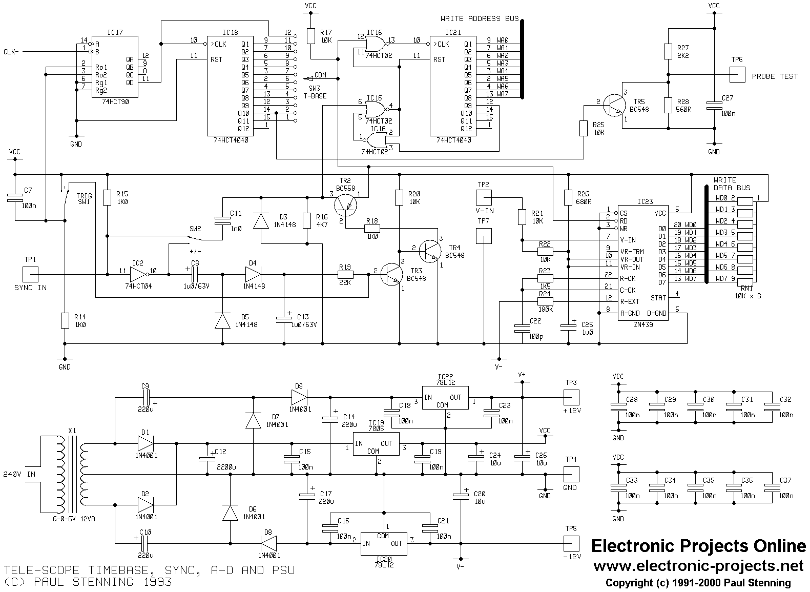
Sync
Assume SW2 (Sync Mode) is in the central position (Normal).
The SYNC signal from the input PCB is pulled up by R15 since it is open collector, and fed to an inverter in IC2. SW2 enables selection of either positive or negative edge triggering. If pulses are present, C13 will be charged, switching TR3 on, which in turn switches TR4 and TR5 off. The rising edges of the sync pulses pass to pin 6 of IC16 via C11.
If there were no sync pulses TR3 would turn off, switching on TR4 and TR5, which couples the timebase frequency to pin 6 of IC16. This results in a free running sync. This would also occur if SW2 was set such that TR3 base is grounded via R14 (Free Run position).
The three gates of IC16 between IC18 and IC21 form a simple S-R flip-flop. This is set to one state by the signals to pin 6 from the sync circuit, and to the other state by the end of a scan (pin 12 of IC21 going high). The first state enables the timebase clock to pass to IC21 whilst the second state holds IC21 reset.
If SW2 is set to the third position (Hold), IC17 is held reset. This disables the timebase and A-D, resulting in a frozen display.
One of the outputs of IC18 is buffered by TR5 and attenuated by R27 and R28 to produce the probe test output.
Power Supply
The majority of the circuit requires a supply of 5V at about 0.5 amps. In addition the input PCB and the A-D require +/- 12V at a few milliamps.
The output of transformer X1 is full wave rectified by D1 and D2, and smoothed by C12, producing about 8.5V DC which is fed to the 5V regulator IC19.
In addition, one output from the transformer is half wave rectified and voltage doubled by D7, D9, C9 and C14, producing about 16V to drive the +12V regulator IC22. A similar arrangement is used to produce the -12V.
Thus the three voltages are derived from one standard transformer. This should be rated at 12VA or greater, since a lower rated unit may not have good adequate regulation for this arrangement to work.
No mains switch or fuse were fitted on the prototype for simplicity, a 3A fuse was fitted in the mains plug.
How it Works - Input Circuit
This is contained on a separate PCB to enable screening if necessary.
The input first passes to the switched attenuator, the input impedance of which is approximately 1M0. The output of the attenuator will be 80mV pk-pk for full scale (10mV/div).
This passes to IC1 which is configured as a unity gain buffer with very high input impedance. An offset null control is provided to ensure that the output is exactly zero volts with the input shorted.
The signal then passes to IC2, the gain of which is set to about 62 and is trimmable by VR2. This amplifies the 80mV pk-pk to 5V pk-pk, which is the full range of the A-D. SW3 shorts the input of this amplifier to ground for base line adjustment. The circuit around the second part of IC2 allows for base line position adjustment. This stage also inverts the signal, for the reason mentioned previously.
IC3 is a comparator which is used to generate the sync pulses. The trigger level is set by VR4, and positive feedback via R26 gives some hysteresis which prevents false triggering on noise.
PCB Construction
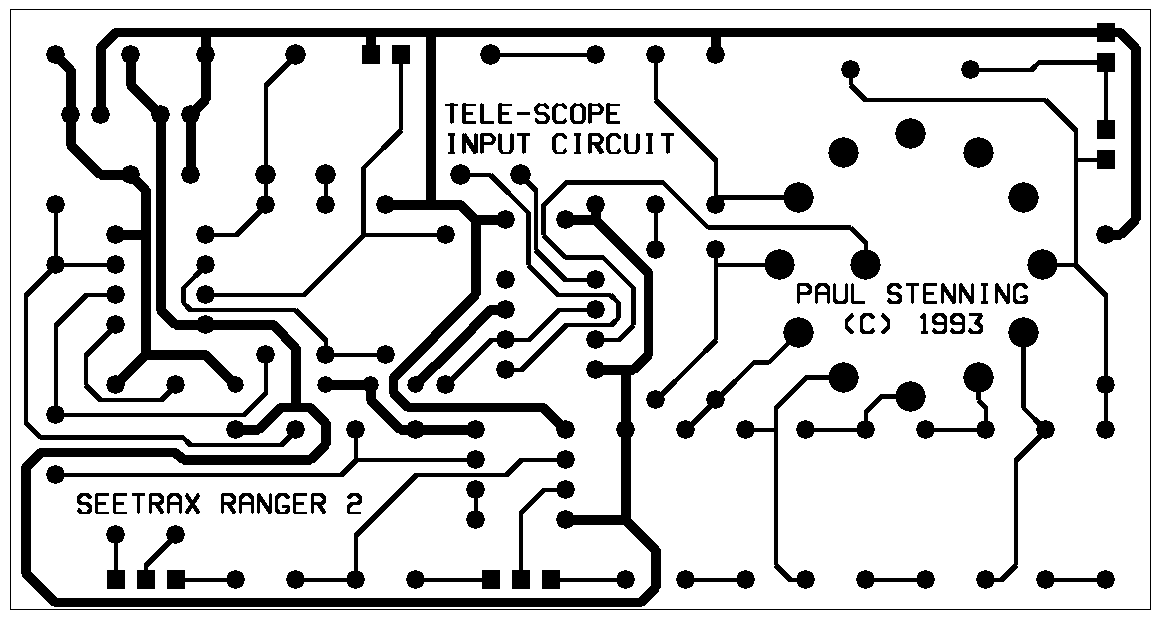
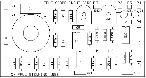
 The input circuit
is constructed on a single sided PCB, 2" x 3.8" in size. The component
overlay is shown in fig ??. Construction is straightforward - do not forget
the two links. IC sockets can be used if desired - one is recommended
for IC1 as this may have to be replaced if an excessive input voltage is applied
to the unit. Veropins should be fitted for the off-board connections.
The input circuit
is constructed on a single sided PCB, 2" x 3.8" in size. The component
overlay is shown in fig ??. Construction is straightforward - do not forget
the two links. IC sockets can be used if desired - one is recommended
for IC1 as this may have to be replaced if an excessive input voltage is applied
to the unit. Veropins should be fitted for the off-board connections.The switch is fitted by cutting the loops from the ends of the pins, the holes in the PCB may have to be enlarged to accommodate the pins. Alternatively short lengths of tinned copper wire may be soldered to the pins and the assembly then fitted to the PCB. The switch stop should be set to allow 8 positions.
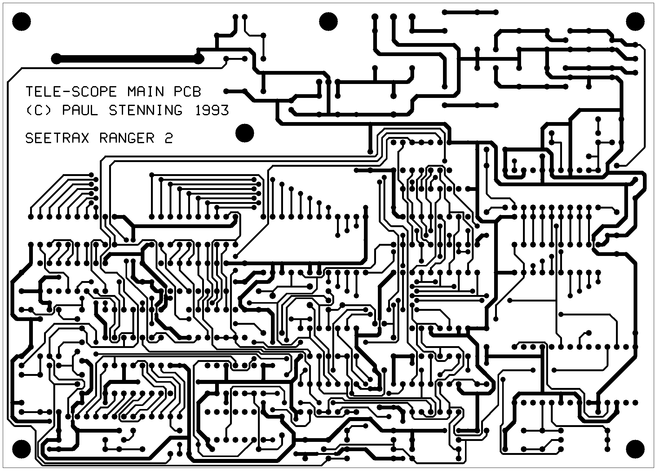
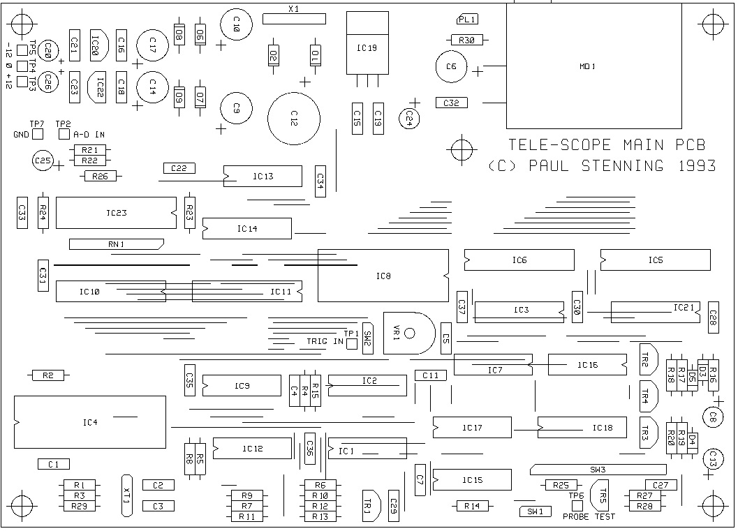
The main circuit is constructed on another single sided PCB, 5" x 7" in size. The component overlay is shown in fig ??.
This board is a little more fiddly to assemble. Firstly the links should be fitted. There are about 80 of these, and some run underneath the bodies of IC's. Thin (about 28SWG) tinned copper wire is recommended for these.
The remaining components can then be fitted, in the usual size order. IC sockets may be used, and are recommended for IC's 4, 8 and 23 since these are more expensive. Veropins or 0.1" header strip connectors should be used for the off-board connections.
If standard 7812 and 7912 devices are used for IC22 and IC23, they should be fitted with their metal tabs towards C21 and C23 (see photo of main PCB).
The 5V regulator (IC19) will run rather warm and a small heatsink or metal bracket should be fitted. Alternatively the regulator could be mounted on a metal panel of the case, and connected to the PCB with short lengths of wire.
Check the PCB very thoroughly after construction, as errors can be difficult to track down with this sort of circuit - particularly if you do not have an oscilloscope!
The Case
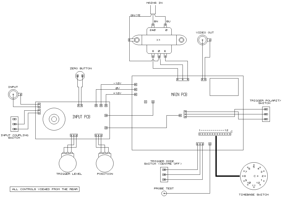
The prototype was housed in a plain aluminum box, 6" x 8" x 2" which was functional whilst not especially elegant. This was also not really large enough, so something slightly bigger would be an advantage. A metal box is preferable for screening, a painted die-cast type may be suitable. There are a number of controls, and it is recomended that a large face on the box is used as the control panel.
The input PCB is mounted on whatever surface is chosen to be the control panel, by the switch mounting nut. The input socket and controls which connect to this PCB should be mounted reasonably close to prevent noise pickup.
This whole input PCB assembly could be screened if required by fitting a suitable diecast box or similar around it. If the base of this box is drilled to match the panel of the case, it can be held in place by the control fixings. This may prove necessary - the prototype showed a little noise on the more sensitive input ranges.
The remaining controls should be positioned away from the input PCB if possible, again to reduce noise. The stop on the Timebase switch should be removed to allow the full 12 positions.
The main PCB should be mounted towards the rear of the case, and a suitable hole drilled for the RF output socket on the modulator. Holes are also required for the video output socket and the mains cable, the latter should be fitted with a cable clip or grommet.
The transformer can be mounted wherever there is room, but it should be well away from the input circuit and the A-D convertor.
The unit can then be wired up as shown in fig ??. The mains connections should be sleeved for safety. Any metal panels on the case, and the 0v rail of the circuit, must be earthed.
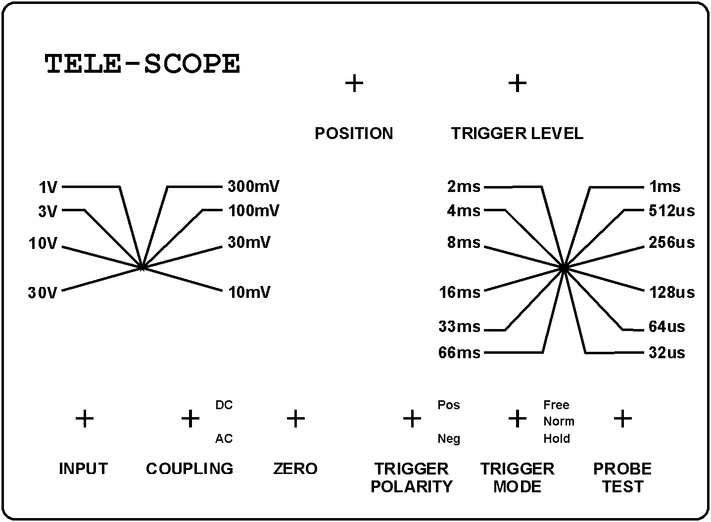
The front panel controls can be labeled as desired. A copy of the prototype artwork is shown in fig ??, this may be photocopied, placed on the case and covered with clear self-adhesive vinal.
Testing
Do not fit any socketed IC's at this stage. Temporarily cover the mains connections with insulation tape if they are not already adequately insulated. Connect to the mains and switch on.
Set your test meter to a suitable DC voltage range, connect the negative probe to TP4 and the positive probe to the pin of IC19 (7805) nearest the modulator. The meter should read 5V DC (+/- 0.25V). Now measure the +12V and -12V supplies on TP3 and TP5, these should both be within +/- 0.5V.
Switch off and insert all the IC's. Set all three presets and both pots to the central positions. Set Input coupling to AC, input range to 3V/div, trigger polarity to +ve, trigger mode to normal and timebase to 8mS/div.
Link the centre pin of the input connector to one of the outer transformer pins on the main PCB, and connect the unit to a TV. Switch on.
Turn the volume on the TV right down, and tune a spare channel selector to channel 36. If all is well (fingers crossed) the graticle and some sort of trace should appear.
The trace should be about 3-4 cycles of an approximate sine wave, but with the top and/or bottom slightly flattened. If the Zero button is pressed it should become a straight line, adjust the position control to place this near the centre line of the graticle if necessary.
Adjust RV1 on the main PCB. The effect obtained will depend upon the make of RAM chip fitted. With RV1 fully anti-clockwise the trace may freeze (this can be confirmed by pushing the Zero button) whilst with the preset fully clockwise, some of the trace dots will be in the wrong positions (this may appear as random dots or more than one trace). Set the preset to a position between these two extremes, which gives a proper trace. Best results were obtained on the prototype using RAM chips made by HMS and Hitachi, although all the devices tried gave acceptable results.
Set the Trigger Mode switch to Hold, and the display should freeze. Now set it to Free Run, and the trace should appear to roll sideways, since the sync is disabled. Return the switch to the Normal position.
Adjust the Trigger Level control, the trace should appear to move sideways as the circuit triggers to different points on the waveform. As the control nears the ends of it's range the trace will roll, due to the sync being lost. Return the control to a point where the unit is triggered and set the trigger polarity to -ve. The trace should appear to invert as the trigger circuit is now operating on the falling edge of the waveform.
Check the operation of the Input Range and Timebase switches by operation them two or three positions either way. Do not set the Input Range to the 10mV/div setting as the input signal is large enough to damage the amplifier on this setting.
Disconnect the input from the transformer, and short circuit the input. Press the Zero button and adjust the Position control to place the line exactly on the centre line of the graticle. Release the Zero button and adjust preset VR1 on the input PCB to bring the trace back onto the centre line. Continue to trim VR1 until the trace does not move when the Zero button is operated.
The best way to adjust the input gain preset (VR2 on input PCB) is by comparison with another oscilloscope, however the following information assumes you do not have this luxury. Set the Input Range to 3V/div, input coupling to DC, and connect the input to TP3 on the main PCB (+12V). Press the Zero button and position the line on the second graticle line up from the bottom. Release the button and adjust VR2 to position the line exactly 4 divisions up from it's previous position. If you have a reasonably accurate meter, measure the +12V and set VR2 accordingly. Disconnect the input.
Finally set the Timebase to 256uS/div and the Input Range to 300mV/div. Connect the input to the probe test output, the display should show about 2 cycles of a square wave, 1 Volt (3.3 divisions) high, above 0V. Switch the input coupling to AC and the trace will drop down the screen about 1.6 divisions.
If you have access to an audio signal generator you can now try the unit on all Timebase and Input Range settings. Take care not to apply more than +/- 10V on the 10mV/div range.
If you've got through all this successfully, the unit is working and set up correctly. In addition you will hopefully have begun to get the feel of using the equipment!
In Use
This is not the place for a full description of the use of an oscilloscope. If the equipment is new to you, a number of books are available, as well as recent magazine articles.
Much of the usage of this unit has been covered in the previous sections, however the following information should be borne in mind.
The maximum frequency signal that can be successfully displayed is 20KHz.
The input is not fully protected against overload. On the 10mV/div range the input signal is applied directly to the op-amp, and therefore must not exceed +/- 10V. On other ranges the attenuator will give some protection, unless the input is excessive. It is generally safest to start on a high voltage range and switch down until a suitable display is obtained.
The ground of the unit is connected to mains earth. Therefore the input must not be connected directly to the mains or to mains powered equipment, unless an isolating transformer is used on the equipment being tested.
AC input coupling is generally used to display a signal which has a DC offset. A good example of this is viewing the ripple on a power supply's output - this may be only a few millivolts but offset by 5 volts or more. Note that the AC coupling capacitor is rated at 250V DC and this must never be exceeded.
The Trigger Mode switch would generally be left in the Normal position, since this will cause the display to free run if it cannot trigger. If measuring static or slow moving DC voltages it may be better to switch to Free Run, to eliminate jitter as the voltage passes the trigger point.
Switching the Trigger Mode to Hold freezes the display, so the probe may be removed. This can be useful if you cannot see the screen and the probe position at the same time. It may also be useful for catching transients and edges, but this relies on you operating the switch at the right moment.
The TV set used may not show the full width of the display. This is not generally a problem, although the set's width control could be adjusted to suit, if one exists. Alternatively it may be possible to move the display from side to side slightly with one of the hold controls, in which case adjust it so the left edge can be seen. These adjustments should only be carried out using external controls if they exist, do not dismantle a TV set unless you are absolutely sure you know what you are doing.
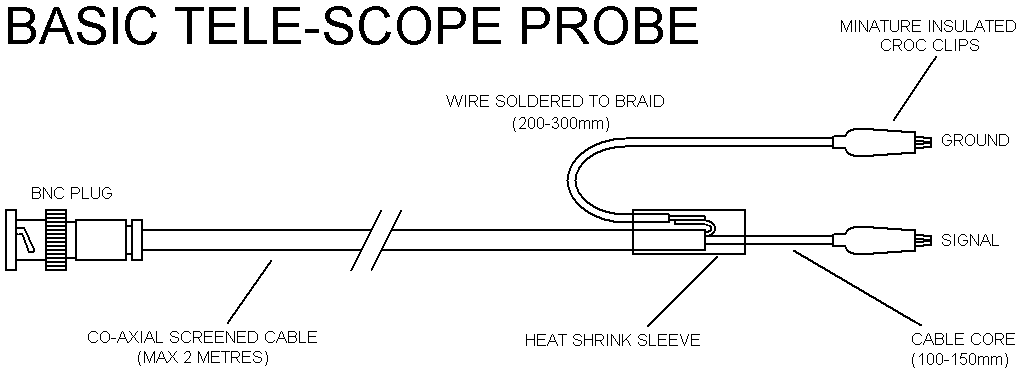
For most purposes an adequate probe can be made using a length of reasonable quality co-axial screened cable about 1.5 metres long with a BNC plug on one end and two small crocodile clips on the other. The clip on the core of the cable could be replaced with a purchased or home made probe of some description if preferred.
The probe test output is used for adjusting X10 and X100 attenuator probes. The probe tip is connected to the output and the adjustment screw on the probe or connector body is adjusted for the best square wave. The leaflet supplied with the probe will give more information.
The Timebase switch offers the following times per division:- 65.536mS, 32.768mS, 16.384mS, 8.192mS, 4.096mS, 2.048mS, 1.024mS, 512uS, 256uS, 128uS, 64uS and 32uS. These are rounded to slightly more tidy numbers on the front panel overlay.
The Input Range offers the following voltages per division:- 30V, 10V, 3V, 1V, 300mV, 100mV, 30mV, 10mV.
Parts List - Input Circuit
All resistors 0.25W, 5% or better.
1% recommended for R1-13.
R1 6M8
R2,3 390K
R4,5 39K
R6,7 3K9
R8,9 390R
R10 270K
R11,18,19 27K
R12 2K7
R13 330R
R14 4K7
R15,17,20-22,25 1K0
R16 56K
R23,24 15K
R26 10K
VR1,2 10K Horizontal Preset
VR3,4 10K Lin Rotary Pot
C1 100n 250V (0.4" lead pitch)
C2,3 10u 25V Radial
C4,5 100n
IC1 CA3140 or CA3160
IC2 LF353N
IC3 LM311
PL1 BNC Socket
SW1 SPST Min Toggle
SW2 1 Pole 12 Way Rotary Make Before Break (S)
SW3 Push To Make Switch
Parts List - Main Circuit
All resistors 0.25W, 5% or better.
R1 3M3
R2,12,16 4K7
R3,5-7,14,15,18,29,30 1K0
R4,28 560R
R8 8K2
R9,26 680R
R10 6K8
R11 3K3
R17,20-22,25 10K
R13 150R
R19 22K
R23 1K5
R24 180K
R27 2K2
RN1 10K x 8 SIL Resistor Network
VR1 1K0 Horizontal Preset
C1,7,15,16,18,19,21,
C23,27-37 100n
C2,3,5 47p
C4 22p
C6 100u 16V Radial
C8,13,25 1u0 63V Radial
C9,10,14,17 220u 25V Radial
C11 1n0
C12 2200u 16V Radial
C20,24,26 10u 25V Radial
C22 100p
XT1 5.000 MHz, HC18U case
TR1,3-5 BC548 or equiv
TR2 BC558 or equiv
D1,2,6-9 1N4001
D3-5 1N4148
IC1 74HCT00 or 74LS00
IC2 74HCT04 or 74LS04
IC3,14,18,21 74HCT4040
IC4 SAA1043
IC5,6,10 74HCT541 or 74LS541
IC7,13 74HCT4078
IC8 6116 2K x 8 RAM 150nS
IC9 74HCT74 or 74LS74
IC11 74HCT688 or 74LS688
IC12,16 74HCT02 or 74LS02
IC15 74HCT4024
IC17 74LS90
IC19 7805
IC20 79L12 or 7912
IC22 78L12 or 7812
IC23 ZN439
PL1 BNC Socket
TP6 1mm Socket
SW1 SPST Centre Off Toggle
SW2 SPST Toggle
SW3 1 Pole 12 Way Rotary Break Before Make (NS)
MD1 UM1233 UHF Modulator
X1 Transformer 6-0-6V, 12VA or greater
Veropins and/or SIL header strip, IC sockets if desired (3 x 8 way, 9 x 14 way, 4 x 16 way, 4 x 20 way, 1 x 22 way 0.4", 2 x 24 way), Thin tinned copper wire, Case, Heatsink or bracket for IC19, 5 Knobs, 3 Amp 3 core mains flex, 13A mains plug with 3A fuse, Cable clamp or grommet, Oscilloscope probe or parts, Phono to Aerial UHF lead, Wire, PCB and transformer mounting hardware.
Buylines
All the non-polarised capacitors except the 100n 250V, should have a 0.2" (5mm) lead pitch. Other types may fit if the leads are formed to suit.
The 74 series logic IC's may be either 74LS or 74HCT; if you are ordering specify the 74HCT. The 4040 and 4024 however must be the 74HCT types, as standard 4000 series devices are not fast enough.
The 78L12 and 79L12 regulators may be replaced with standard 7812 and 7912 types, if these are to hand.
The two rotary switches are identical in appearance. For identification, the Make Before Break is marked "S" on the base, whereas the Break Before Make is marked "NS".