The unit presented here will emulate the standard 27 family of devices, from 2764 to 27512, and can be used with an IBM PC compatible computer. The smaller 24 pin devices in this family (2708, 2716 and 2732) are almost obsolete and are now more expensive than a 2764. I did not feel it necessary to accommodate these devices in this design since they would significantly increase the complexity.
 This design uses
readily available components to reduce the likelihood of obsolescence.
The unit is powered from either an external PSU or the circuit under development
- the supply requirement being 5V @ 100mA. The power supply design for
the EPROM Programmer will also power this unit if an external supply is needed.
This design uses
readily available components to reduce the likelihood of obsolescence.
The unit is powered from either an external PSU or the circuit under development
- the supply requirement being 5V @ 100mA. The power supply design for
the EPROM Programmer will also power this unit if an external supply is needed.The emulator itself is dumb and is controlled by the host computer via the RS232 serial port (COM1 or COM2). Device selection and operation mode is set by front panel switches.
The accompanying software is available for download. The software will operate on any PC running MS-DOS or PC-DOS version 3.0 or later and having at least 512K of RAM and one RS232 serial port. A hard disk and a colour monitor are strongly recommended. The software is written in Microsoft QuickBASIC V4.5, and the full source code is supplied for those wishing to enhance or modify it. This source code is also compatible with QBASIC, as supplied with MS-DOS 5.0 and later. You do not need QuickBASIC or QBASIC to use this disk. The disk also contains the software for the EPROM Programmer. A description of the software operation is given later.
The unit may also be suitable for use with other types of home computer having an RS232 serial port, although this has not been tested and no software is available. It will definitely not work with Commodore Amiga computers, due to a peculiarity in the serial port handling.
How it Works
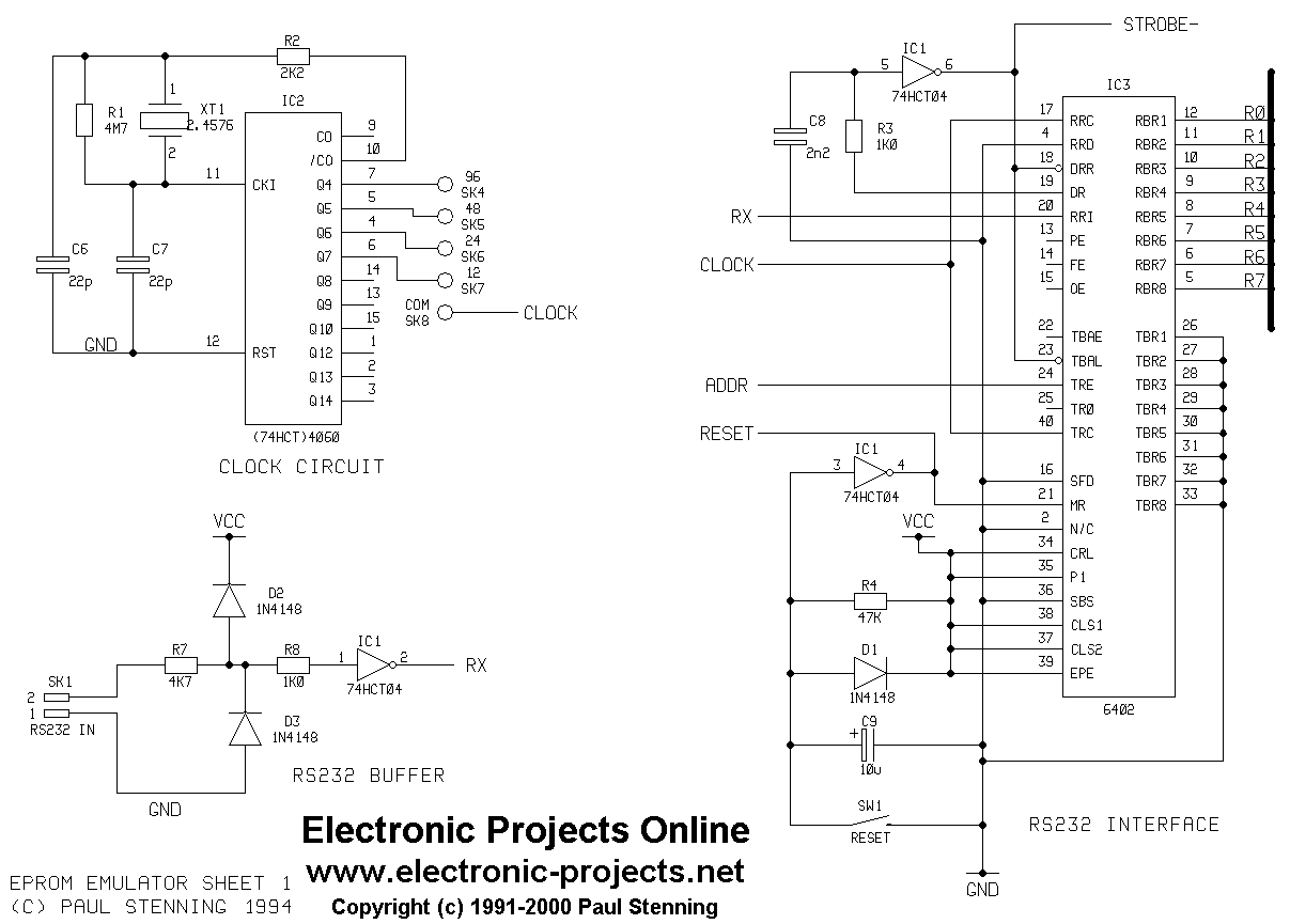
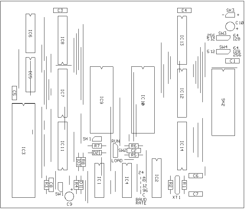
The circuit diagram is spread over a number of illustrations. Although it may initially look complex, it is in fact relatively straightforward. When a "-" follows a signal name (for example STROBE-), this shows that the line is active low. When a number is followed by an "h" this indicates that the number is hexadecimal.
The RS232 (serial) interface, buffering and clock are shown in figure *. IC3 (6402) is a UART (Universal Asynchronous Receiver/Transmitter) which basically converts serial data to parallel and vice-versa. The device supports most common serial data formats, in this application it is configured to give eight data bits, one stop bit and no parity checking. The data rate is set by the crystal controlled clock circuit (IC2), which in most cases will be set to 9600 Baud. Since this unit is designed to receive data only, the parallel input lines (pins 26 to 33) are held low and the serial data output line (pin 25) is not connected.
A gate in IC1 is used as the RS232 buffer, converting the +/- 10V RS232 standard data from the PC to a 5V pulse train suitable for the UART. The diodes restrict the RS232 voltage to within the 0-5V range, the remainder is dropped across R7.
A byte of serial data arriving on pin 20 of IC3 will be converted to parallel data, which will appear on pins 5 to 12. Pin 19 will go high, and no further data can be received until pin 18 is taken low momentarily. One gate of IC4 causes this to happen, R3 and C8 create a slight delay giving a STROBE- pulse with adequate width for clocking other devices.
R4, D1, C9 and one gate of IC4 produce the power-on reset pulse for IC3, IC5 and IC6. SW1 allows the circuit to be reset again as required.
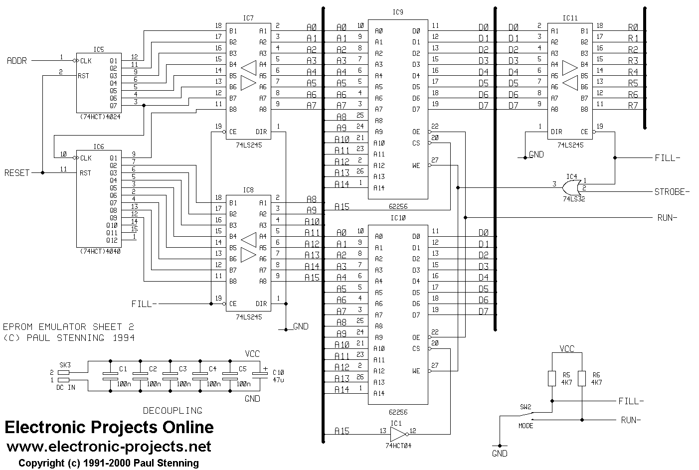
Assume SW2 is in the upper position (Upload), so Fill- is low and Run- is high. IC12, IC13 and IC14 are disabled, so the 'EPROM' socket SK1 is isolated from the RAM. IC7, IC8 and IC11 are all enabled, effectively connecting the RAM (IC9 and IC10) to the address counters (IC5 and IC6) and the UART.
When a byte of data is received, the Strobe- line will pulse low as described previously. This is connected to the Write Enable- (pin 27) on the RAM IC's so the received data will be written to the current memory location.
The Strobe- signal is also connected to pin 23 of the UART. This will cause the transmission section of the device to go through it's motions (even though nothing is listening!). As the data is sent, pin 24 will pulse, incrementing the address counters IC5 and IC6. The section of the UART is used to merely apply a suitable delay before the address is incremented, to ensure the data is correctly stored.
When the next byte of data is received, it will be loaded into the next memory location, and so on. As long as the user presses the Reset button when prompted by the software, the data will arrive in the correct places. The software simply sends the data to the emulator one byte at a time, you could alternatively simply copy a binary image file to the COM port.
Two 256K x 1 Bit (32K x 8 Bit) RAM devices are used, to obtain the full 64K addressing range of a 27512 EPROM. The CS lines are used in conjunction with an inverter on the A15 line to select which device is used at a particular time.
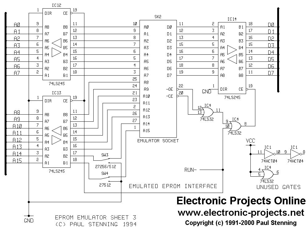
Now assume that SW2 is in the lower (Run) position. IC7, IC8 and IC11 are now disabled, isolating the RAM from the upload circuitry. IC12 and IC13 are enabled, effectively connecting the RAM address bus to the 'EPROM' socket. SW3 and SW4 select the EPROM type, and set any unused RAM address lines low. When pins 22 and 24 of the 'EPROM' are both low, IC14 is enabled (via IC4) connecting the RAM data lines to the 'EPROM'.
The prototype has not yet been tested on a speed-critical microprocessor system. The interface electronics should add no more than 20ns to the access time of the RAM devices used. Therefore with 100ns RAM chips, the unit should be able to emulate a 120ns EPROM, and will definitely emulate a 150ns device. If speed is critical, fit the fastest RAM chips you can get - 35ns devices are available if you are prepared to pay for them!
Construction
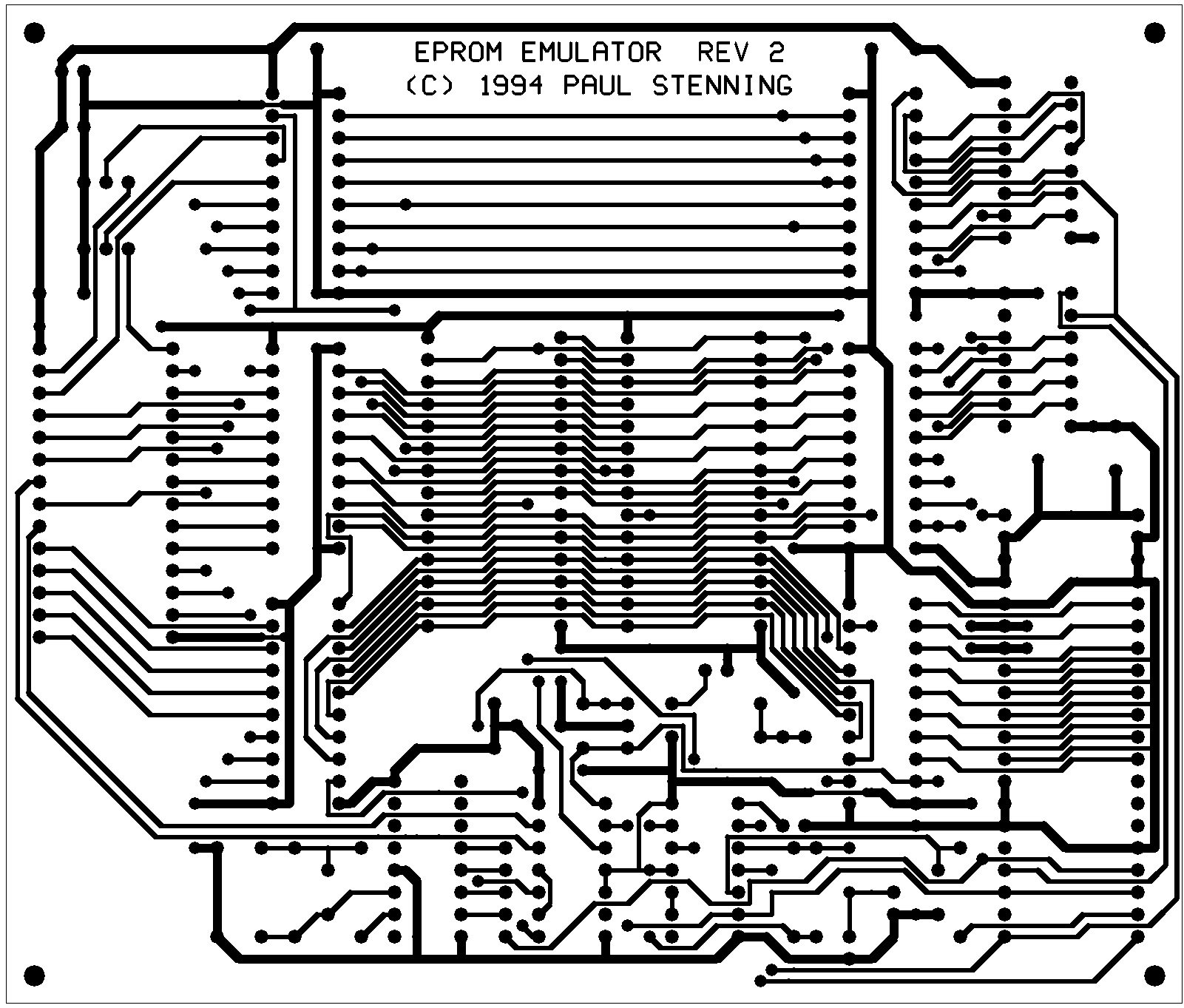
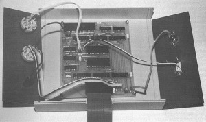
The unit is assembled on a single sided PCB. A number of wire links are required, which should be fitted before any components, since some pass underneath ICs. I would suggest that the resistors are fitted next, followed by the ICs, then the capacitors, then the remaining parts. Fit a link wire between COM and 96 to set the Baud rate to 9600. Fit SIL header strip or Veropins for the off-board connections.
 I would suggest that
sockets are used for the RAM chips and the UART, in view of their cost.
It would also be a good idea to use sockets for IC4, IC12, IC13 and IC14, since
these interface to the outside world and could be damaged if there is a problem
on the system being tested. The sockets allow for ease of changing if
the worst happens.
I would suggest that
sockets are used for the RAM chips and the UART, in view of their cost.
It would also be a good idea to use sockets for IC4, IC12, IC13 and IC14, since
these interface to the outside world and could be damaged if there is a problem
on the system being tested. The sockets allow for ease of changing if
the worst happens.If you do not plan to emulate 27512 EPROMs, you could save a few pounds by omitting IC10 (it can always be added later). The unit will then emulate up to 27256 devices, so move the stop on the Device switch to prevent the 27512 option being selected.
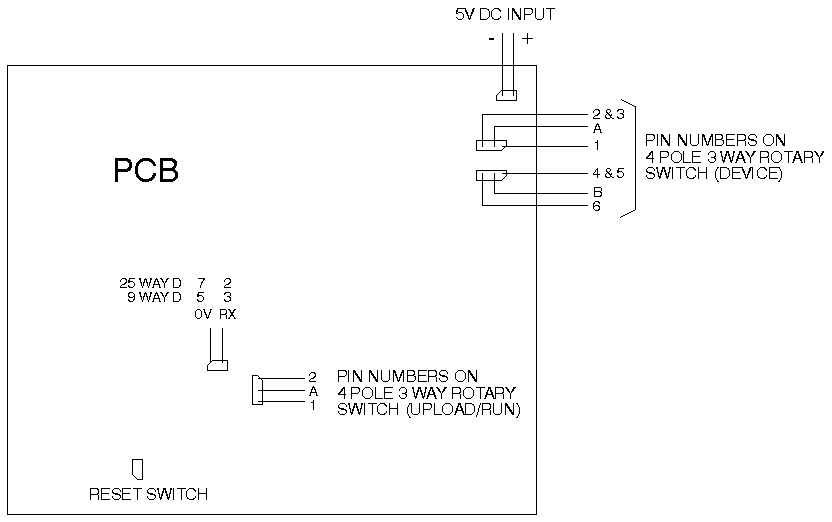
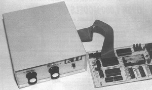
Fit a 28-way IC socket in SK2 position. A 300mm (or shorter) length of 28 way ribbon cable should be fitted with a 28 way DIL connector on each end. These can be readily pressed together in a vice or WorkMate, if three thicknesses of Veroboard are used to protect the connector pins. Take care when doing this, as it is not easy to get the connector apart again if something goes wrong. One end of this cable plugs onto SK2, make sure the edge of the cable with the different colour goes to pin 1.
When you receive these connectors from your supplier, please make sure the two parts are not pressed fully together before removing from the polythene packing. If they are, send them back. The two I purchased from Maplin were fully assembled and I managed to break one while disassembling them.
The interwiring is shown in figure *. This should be carried out at this stage, since it is necessary for testing. After testing the board can be fitted into the case.
The connections for both 9 and 25 way serial connectors, use whatever matches the socket on your computer. On the prototype a 9 way D connector (serial) and a 6 way DIN socket (DC input) were fitted to the case. The rotary switch connections are shown by giving the pin number or letter marked on the switch body.
Testing
Connect the unit to a 5V supply and the serial port on your PC, and run the program "SER-TEST.EXE" on the software disk. When prompted, type "1" or "2" followed by <Enter> to say which serial port you are using. The program does nothing more exciting than wait for you to enter a 2-digit hex number (followed by <Enter>) and then sends it to the emulator. It then attempts to read back a number, if it's successful it prints the number otherwise it prints "**". Since the emulator does not transmitt any data the software will always respond with "**". To exit just press <Enter> on it's own. All the responses in this section will be shown with quotes ("") around them - just type the number (followed by <Enter>), don't type the quotes.
Switch the emulator to 27512 and Upload, and press Reset. Type "00" on the computer, and the software should respond with "**". Using a logic probe, test meter or oscilloscope, check the logic levels on pins 9, 10, 11, 13, 14, 15, 16 and 17 of IC9. They should all be low. If you type "01", pin 9 should be high, and the others should remain low. Now enter "02", "04", "08", "10", "20", "40" and "80" in turn. After each entry, check the logic levels on the data pins, only one should be high in each case - 10, 11, 13, 14, 15, 16 and respectively.
Press Reset on the programmer. Press Enter on it's own to quit the software then run "ADR-TEST.EXE", which is also on the disk. Since the address counters are incremented when a byte is sent, it would take a long time to get the count to 65535 manually! ADR-TEST does it automatically, and pauses at four points to allow you to check the logic levels. Follow the instructions on screen. The table below shows the expected logic levels on the address pins of the IC9 at the four pause points.
-----------------------------------------------------------------------------
Addr Line A15 A14 A13 A12 A11 A10 A9 A8 A7 A6 A5 A4 A3 A2 A1 A0
IC9 Pin 20 27 26 2 23 21 24 25 3 4 5 6 7 8 9 10
-----------------------------------------------------------------------------
Count Expected Logic Level
0 0 0 0 0 0 0 0 0 0 0 0 0 0 0 0 0
21845 0 1 0 1 0 1 0 1 0 1 0 1 0 1 0 1
43690 1 0 1 0 1 0 1 0 1 0 1 0 1 0 1 0
65535 1 1 1 1 1 1 1 1 1 1 1 1 1 1 1 1
-----------------------------------------------------------------------------
If these readings are OK, and the preceding tests were also successful you can be fairly confident that the unit is working correctly. It is not so easy to check emulation part of the unit, but providing the unit was carefully constructed the chances of problems are unlikely.
If you have a microprocessor system and a suitable hex file , you can try emulating a known good EPROM using the information given shortly.
The Case
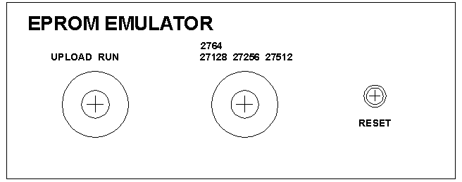
The prototype was constructed in a plastic case, 190mm x 165mm x 68mm, see parts list for details. A suitable overlay for the front panel is shown in figure *. Two photocopies may be taken (enlarge to 162mm x 64mm), one can then be used as a drilling template while the other may fixed to the front panel with clear self-adhesive vinyl.
A suitable notch should be cut in the right side of the case for the ribbon cable to pass through. The power and RS232 connectors mount on the rear panel.
Software