An exact specification was not offered, they felt that almost anything would be better than the existing system. We decided that about half a second between echoes would be more than adequate for a maximum delay range. The shortest delay is so fast that sounds resembling microphone feedback can be obtained. Metallic alien reverberations similar to those on the "Smash" instant potato television adverts are also possible.
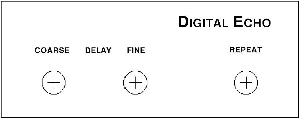
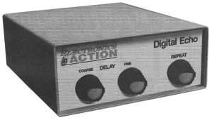 Simplicity of operation
is essential for the intended use. Consequently, there are only
three controls on the front panel. Two of these set the delay required
(coarse and fine). The third is the Repeat control, which sets the
amount of echo signal fed back around the loop. This ranges from 0% to
almost 100%.
Simplicity of operation
is essential for the intended use. Consequently, there are only
three controls on the front panel. Two of these set the delay required
(coarse and fine). The third is the Repeat control, which sets the
amount of echo signal fed back around the loop. This ranges from 0% to
almost 100%.My original plan was to use bucket brigade delay line chips, however several devices would have been necessary to cover the required delay at a reasonable frequency bandwidth. Significant distortion can also result as the voltage samples are passed down the chain.
The design presented here uses an 8K RAM chip to store the data samples. The delay of half a second is achievable, with a bandwidth of 8KHz. The incoming signal passes through with no bandwidth limiting. Distortion on the echo signals is generally less than 5%, although this will build up each time a sound is echoed.
The upper frequencies would normally be lost on natural echos, so the bandwidth limitation is not a problem in practice. Similarly the distortion on the echo signals will generally pass unnoticed.
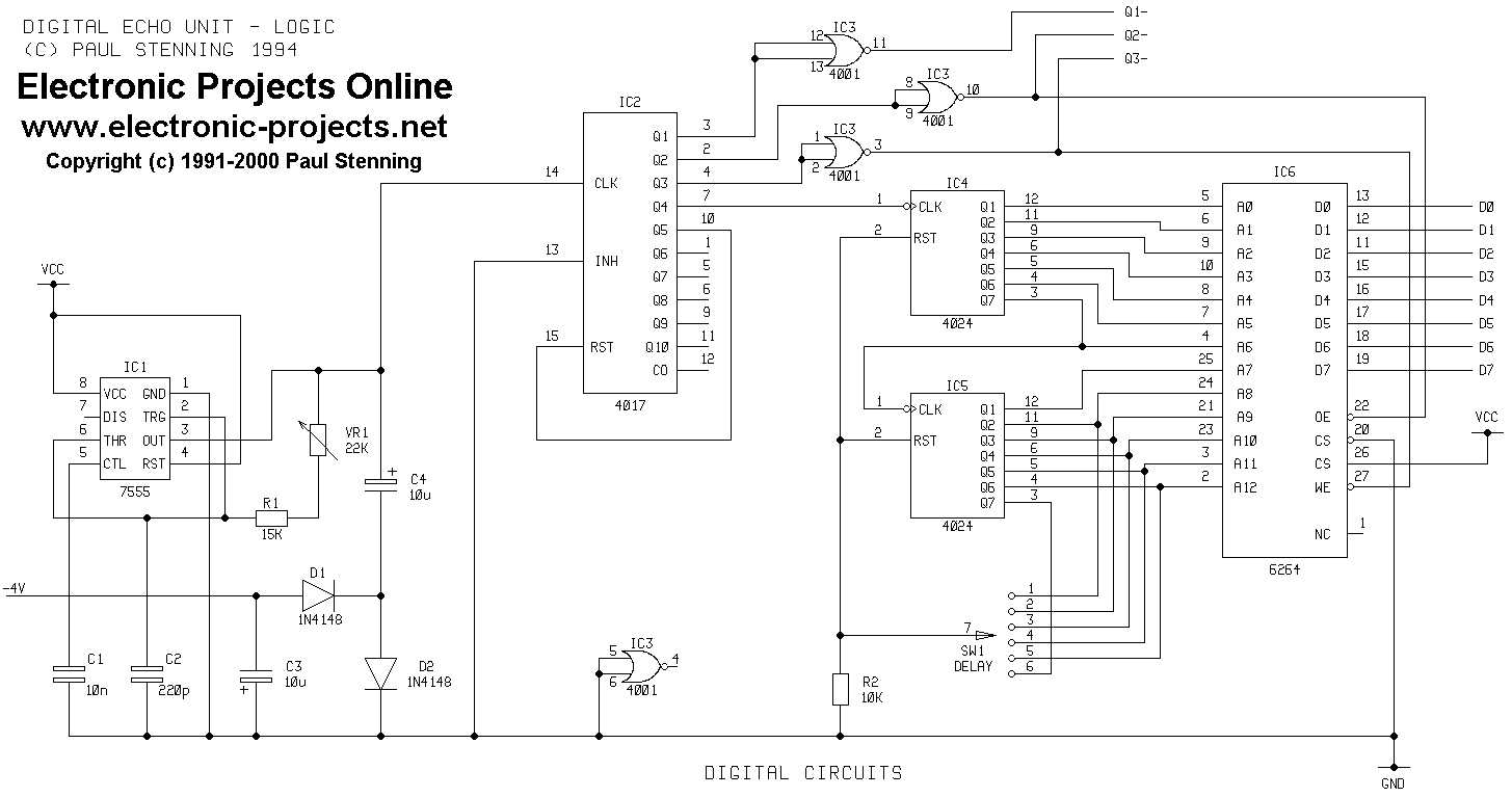
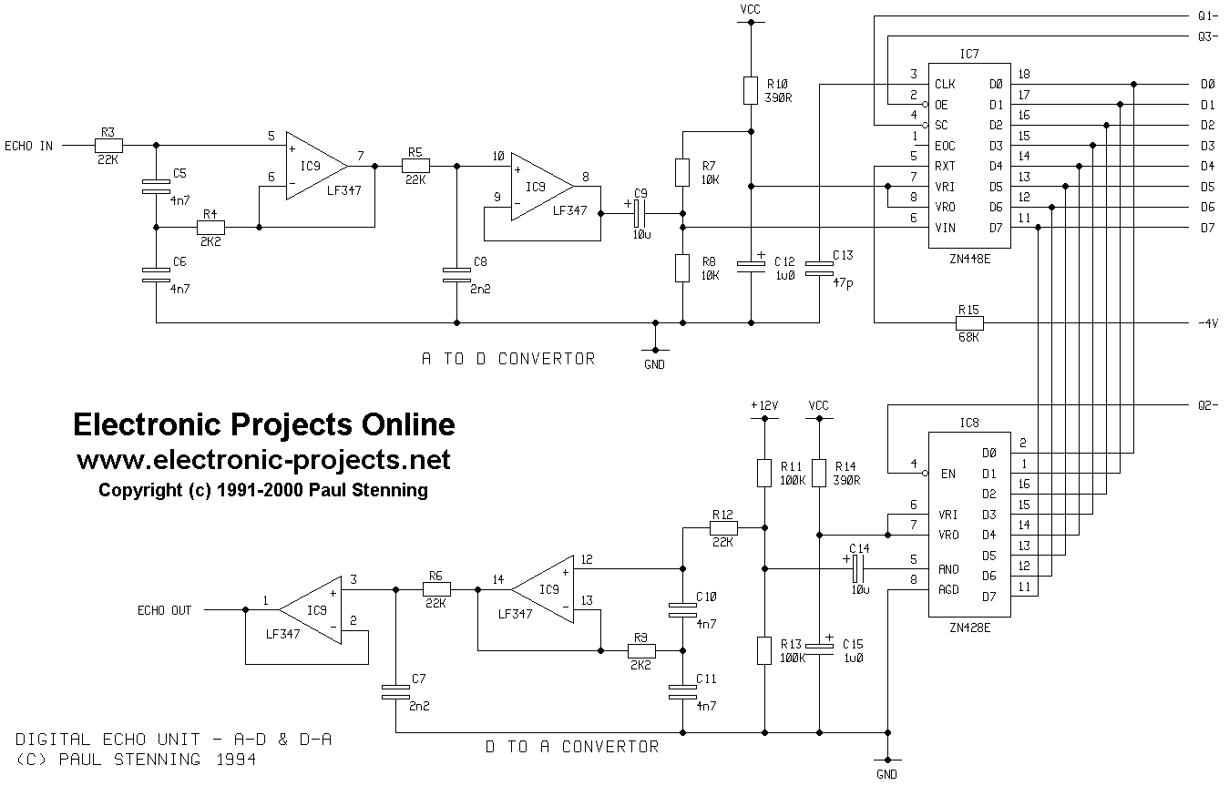
The Works
The complete circuit diagram appears in figures ** and **.
Starting with the digital section. IC1 is the clock generator, which runs at four times the sampling frequency. The frequency is adjustable over a limited range by VR1, the Delay Fine control. This slightly unusual configuration gives an output with an approximately equal mark-space ratio.
The A-D convertor IC7, requires a negative bias on pin five. Since the current required in minimal, this negative voltage is obtained by rectifying the clock signal from IC1, giving approximately -4V.
IC2 produces the four timing pulses required, three of which are inverted by gates in IC3. When Q1 goes high, the A-D convertor IC7 starts a conversion. When Q2 is high, the data in the RAM is sent to the D-A convertor IC8, which produces the appropriate voltage. When Q3 is high, the data from the A-D is stored in RAM. Finally when Q4 pulses high, the address counters IC4 and IC5 are incremented.
SW2 (Delay Coarse) sets the count reached by the address counters before they are reset. This sets the amount of the RAM chip to be used.
Ideally I would have had just one continuously variable delay pot, on the 555 clock circuit. However, it was not possible to achieve the required range with a respectable frequency response due to the A-D conversion time.
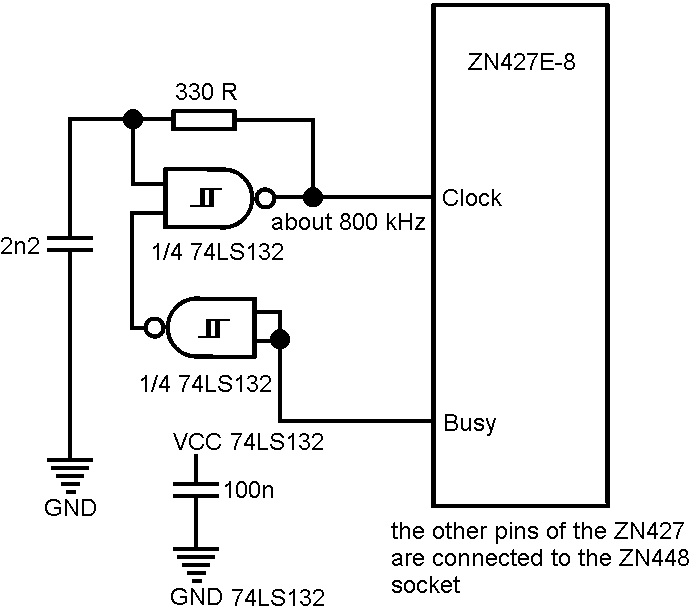
The ZN448E (IC7) is an 8 bit successive approximation A-D convertor. Nine clock cycles are required for each conversion. The eight data lines are tri-state, and controlled by the OE- pin.
The device contains a built in clock circuit, the frequency of which is set by C13. The data sheet gives the maximum clock frequency as 1MHz, and a graph shows that a capacitor value of 100pF will give this. However tests with several devices showed that 100pF gave a frequency of only about 500KHz. To achieve 1MHz a 47pF capacitor is required. It is possible that some ZN448E devices will fail to operate with a 47pF clock capacitor. In which case replace C13 with a 100pF component, or the lowest value that gives correct operation. R10 is the biasing resistor for the internal voltage reference, which is decoupled by C12.
The ZN428E (IC8) is an 8 bit D-A convertor, which uses an R-2R resistor network driven by an accurate voltage reference. This reference is biased by R14 and decoupled by C15. A latch circuit on the data input lines is controlled by the EN- pin. When EN- is inactive, the previous output voltage remains.
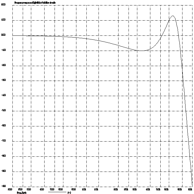
The audio signals to the A-D convertor and from the D-A convertor pass through identical low pass filter circuits. These have a slope of 24dB per octave and a -3dB point at about 8KHz. The frequency response of these filter circuits is shown in figure *. The variation of +/- 1.3dB before the cutoff point is not important in this application.
The filter on the input to the A-D prevents any signals with a frequency too high to be accurately sampled from reaching the convertor. Allowing these signals through would result in severe aliasing distortion, leading to a poor quality output. The filter on the D-A output removes noise due to the sampling frequency, and smooths the stepped output to some extent.
The audio output from the delay circuit is mixed with the input signal by the circuitry around IC10. VR2 sets the amount of signal that is fed back around the system.
The circuit is powered by a 12V 250mA transformer. The required +5V (VCC) and +12V supplies are regulated by standard three pin linear regulator IC's.
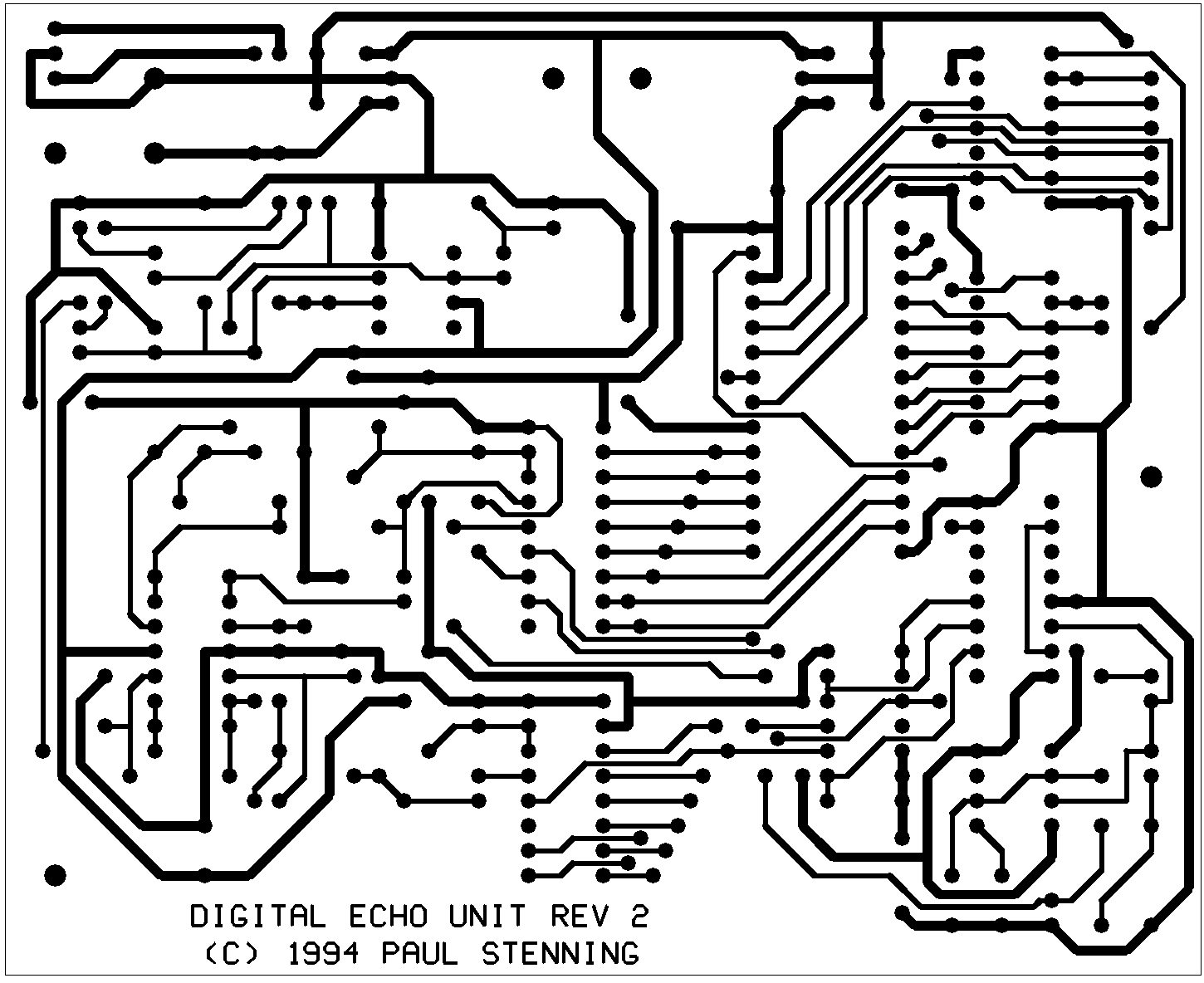
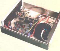
Construction
The circuit is constructed on a single sided PCB. The track layout and component positioning are shown in figure *.
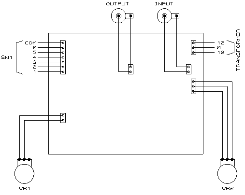
There are 30 links that should be made first, using thin (approx. 26SWG) tinned copper wire. The resistors, diodes and capacitors can then be fitted in size order. Sockets may be used for the IC's if required - since all the devices are static sensitive this may be a good idea. Do not insert the IC's into the sockets until the remainder of the PCB construction is complete.
 IC11 and
IC12 will become warm in operation and should be mounted on a small heatsink.
The mounting tabs of both devices are connected to the 0V rail so no insulation
washers are required. A small amount of silicone grease or heat
transfer paste should be placed between the devices and the heatsink.
IC11 and
IC12 will become warm in operation and should be mounted on a small heatsink.
The mounting tabs of both devices are connected to the 0V rail so no insulation
washers are required. A small amount of silicone grease or heat
transfer paste should be placed between the devices and the heatsink.Terminal pins may be fitted in the holes for the off-board wiring, so that the connections can be made after the PCB is fitted into the case.