 The
ChipTester presented here is used with an IBM compatible PC, and will
test nearly all logic devices, providing they operate from a single 5V
supply and have no more than 24 pins. Devices with over 20 pins
must have the power pins on the usual diagonally opposite corners.
The only logic devices that cannot be tested are those incorporating analog
techniques, such as monostables and phase locked loops.
The
ChipTester presented here is used with an IBM compatible PC, and will
test nearly all logic devices, providing they operate from a single 5V
supply and have no more than 24 pins. Devices with over 20 pins
must have the power pins on the usual diagonally opposite corners.
The only logic devices that cannot be tested are those incorporating analog
techniques, such as monostables and phase locked loops.This system may also be useful for educational establishments, for checking devices removed from students projects before returning them to the stores for reuse.
The accompanying software is available on this website. The software will operate on any PC running MS-DOS or PC-DOS version 3.0 or later and having at least 512K of RAM and one RS232 serial port. A hard disk and a colour monitor are strongly recommended. The software is written in Microsoft QuickBASIC V4.5, and the full source code is supplied for those wishing to enhance or modify it. This source code is also compatible with QBASIC, as supplied with MS-DOS 5.0 and later. Several sample device files for common logic devices are also included.
The software allows the creation of test parameters for new devices, which can be saved to disk. Devices can be tested either once only, or continuously to find intermittent faults. As the tests progress the logic levels on each pin are displayed using colours. A detailed description of the software operation is given later.
The unit may also be suitable for use with other types of home computer having an RS232 serial port, although this has not been tested and no software is available. It will definitely not work with Commodore Amiga computers, due to a peculiarity in the serial port handling.
The Works
The circuit diagram is spread over a number of illustrations. Although it may initially look complex, it is in fact relatively straightforward. When a "-" follows a signal name (for example STROBE-), this shows that the line is active low. When a number is followed by an "h" this indicates that the number is hexadecimal.
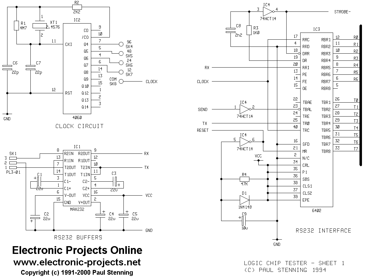
The RS232 (serial) interface, buffering and clock are shown in figure *. IC3 (6402) is a UART (Universal Asynchronous Receiver/Transmitter) which basically converts serial data to parallel and vice-versa. The device supports most common serial data formats, in this application it is configured to give eight data bits, one stop bit and no parity checking. The data rate is set by the crystal controlled clock circuit (IC2), which in most cases will be set to 9600 Baud.
IC1 is the RS232 buffer, converting the 5V data from the UART to the +/- 10V RS232 standard, and vice-versa. This device contains a voltage doubler and voltage invertor circuit, producing +/- 10V rails from a single +5V input. The four external capacitors (C1 to C4) are required for these circuits.
A byte of serial data arriving on pin 20 of IC3 will be converted to parallel data, which will appear on pins 5 to 12. Pin 19 will go high, and no further data can be received until pin 18 is taken low momentarily. One gate of IC4 causes this to happen, R3 and C8 create a slight delay giving the STROBE- pulse adequate width for clocking other devices. When pin 23 is pulsed low, the parallel data on pins 26 to 33 is transmitted in serial form from pin 25. R4, D1, C9 and one gate of IC4 produce the power-on reset pulse for IC3.
Since the device being tested will have more than eight pins, we need a method of connecting the eight input lines and eight output lines on the UART to the 24 pins on the test socket. We also need to arrange for the data to be transmitted by the ChipTester when required.
The data output from the UART is divided into two sections. Lines R0 to R3 are used as four data lines, and lines R4 to R6 are used as three address lines, to control where the four bits of data go to. The eighth output line is not used.
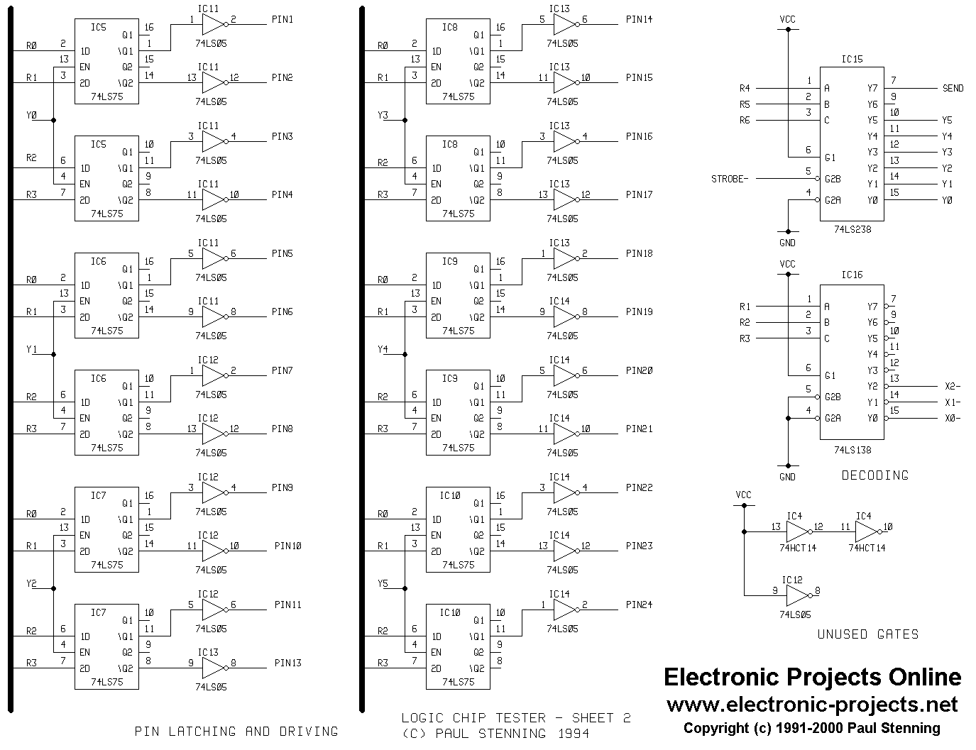
The decoding and output buffering is shown in figure *. The three "address" lines (R4-R6) are decoded by IC15. The STROBE- signal is connected to one of the enable pins so that a short pulse appears on the appropriate output (Y0-Y5). These pulses are used to clock the four data bits into the appropriate 74LS75 latch (IC5 to IC10). Thus, 24 bits of data can be sent in six bytes.
To load data into the first 4 latches, we send 0Xh, where X is the data required. For the other latches the codes are 1Xh to 5Xh.
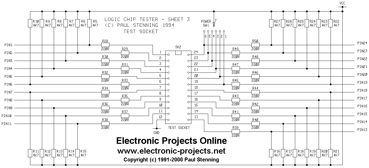
The outputs of the latches are connected to open collector inverting buffers. Open collectors are used since they save us having to differentiate between input and output lines. If the line is set high, it can be used as an input, and pulled low by the device being tested. The pullup 4K7 resistors are shown in figure *. 220R current limiting resistors are used to protect the ChipTester and the device being tested in case of conflict. Only 23 of the 24 outputs are used, pin 12 of the socket is connected directly to 0V. The power to the device under test is set by SW1.
Devices with unusual power pin arrangements are accommodated by placing them one position up from the bottom of the test socket, and linking the power pins with wires. The software will give details when necessary.
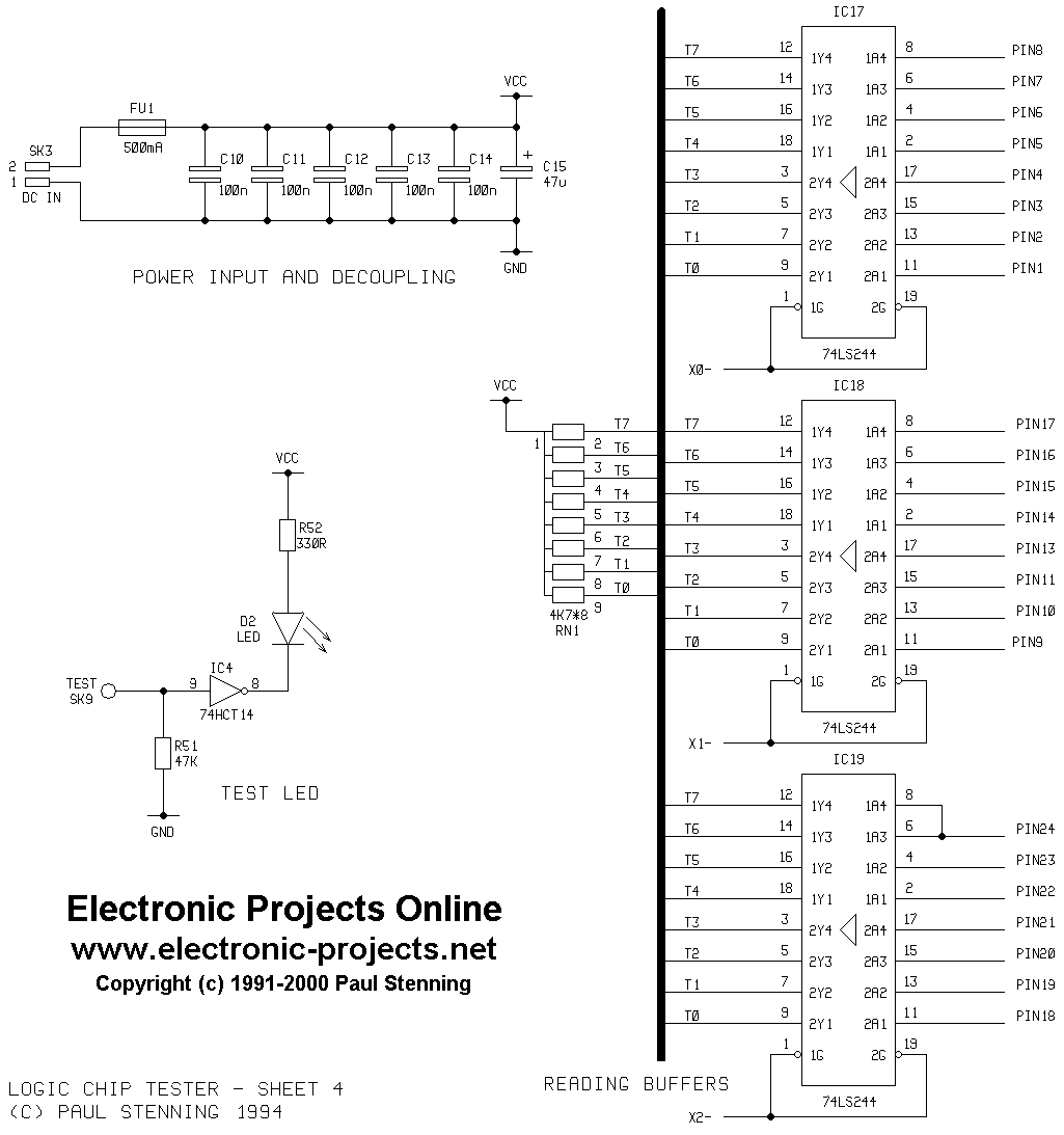
To read back the state of the device pins, they are connected to three tri-state buffers (IC17-IC19), shown in figure *. One of these is selected by IC16, which is connected to three of our "data" lines. A decoding device is used to ensure that no more than one tri-state buffer is selected at a time. RN1 holds the lines high when no buffer is selected.
When output Y7 of IC15 pulses high the appropriate byte is transmitted. Thus to tell the Chiptester to send a byte of data, we send 70h, 71h or 72h, depending upon which 8 bits we need.
A spare gate on IC4 is used as a simple logic probe for testing the unit. When pin 9 is taken high, pin 8 goes high turning on the LED.
The power into the unit is protected by a 500mA fuse, to (hopefully) protect the unit and power supply if the device being tested is internally short-circuited or inserted incorrectly. A separate regulated 5V supply is required - a simple 7805 based circuit will suffice. You may be able to pick up a 5V supply from a spare disk drive connector inside your PC, or from the keyboard connector - but take great care not to cause any damage! The Eprom PSU project on this website is suitable.
Construction
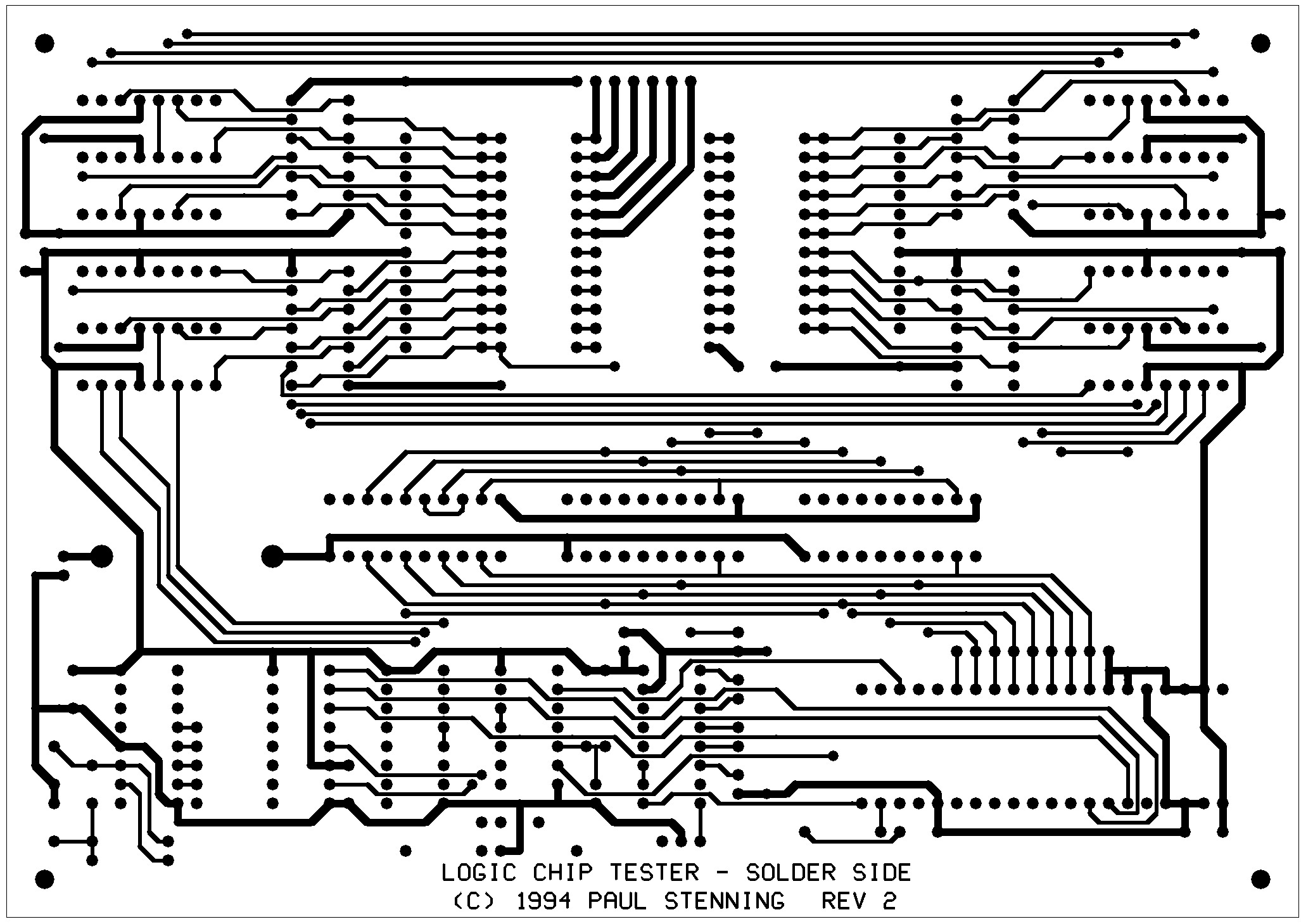
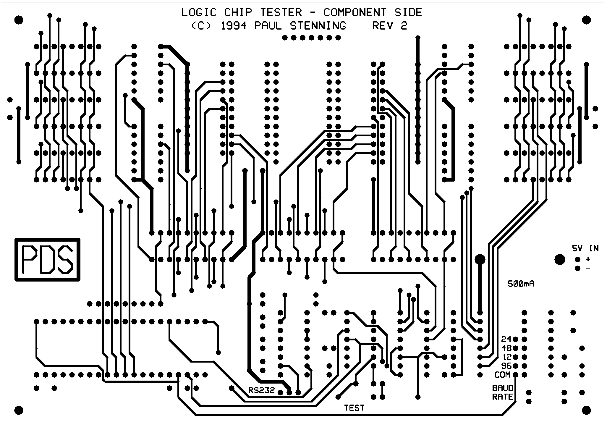
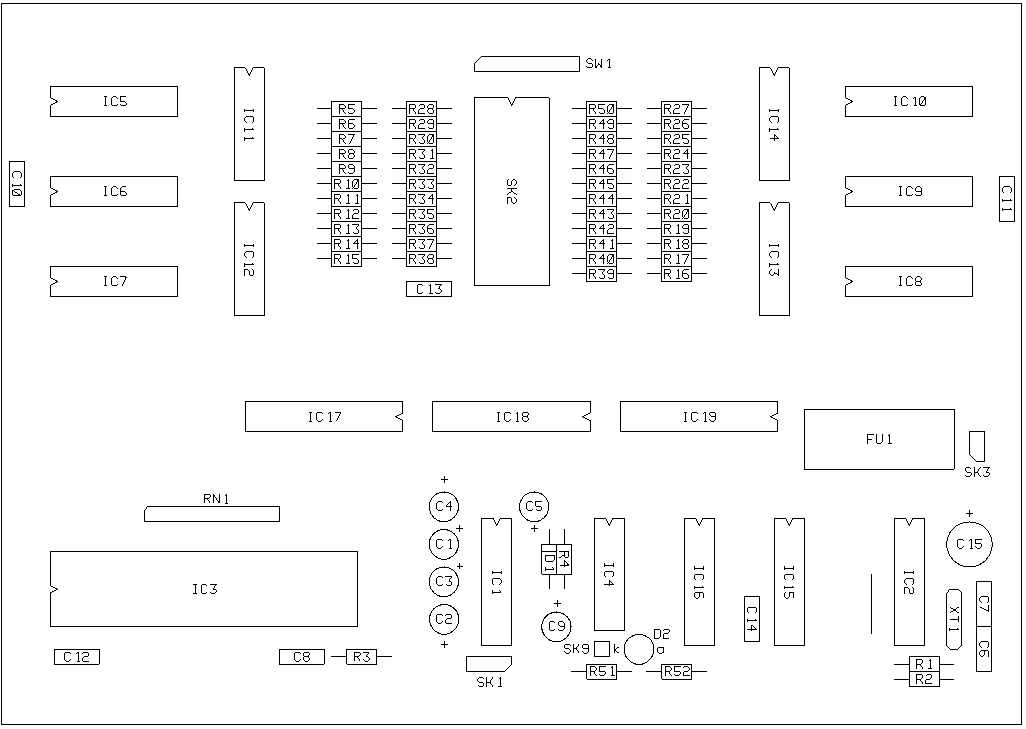
The unit is assembled on a double sided PCB. The copper track layouts are shown in figure * and the component overlay is shown in figure *.
The PCB does not have plated through holes, so you will need to solder some component pins on both sides of the board. Because of this, normal IC sockets cannot be used. Some turned pin sockets have metal showing on the top of the board, alternatively the ICs can be soldered directly into the PCB. There are also several through hole connections that need to be fitted with track pins or short pieces of wire - these are best left until after the components have been fitted.
I would suggest that the resistors (excluding R4) are fitted first, followed by the ICs, then the capacitors, then the remaining parts. Fit a link wire between COM and 96 to set the Baud rate to 9600. Fit SIL header strip or Veropins for the off-board connections.
Fit a 24-way IC socket in the test socket position. Plug two more sockets into this, then plug the ZIF (Zero Insertion Force) socket into the top. If this stack feels unsteady use some Araldite or similar to hold it together. When buying the ZIF socket, be sure to get one with wide slots that will accept 0.3" and 0.6" devices.
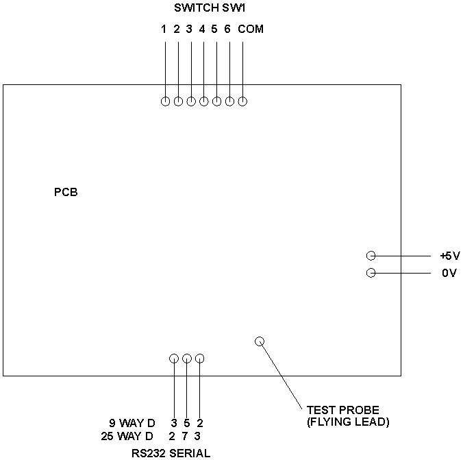
The interwiring is shown in figure *. This should be carried out at this stage, since it is necessary for testing. After testing the board can be fitted into the case.
The connections for both 9 and 25 way serial connectors, use whatever matches the socket on your computer. On the prototype a 9 way D connector (serial) and a 6 way DIN socket (DC input) were fitted to the case.
Connect a length of wire to the test pin, at least long enough to reach pin 1 of the test socket.
Testing
Connect the unit to a 5V supply. If a test meter is to hand, check for about +9V on pin 2 and -9V on pin 6 of IC1 (MAX232). Touch the test lead onto the fuse holder contact to check the tester works - the LED should light!
Connect the unit to the serial port on your PC, and run the program SER-TEST.EXE on the software disk. When prompted, type "1" or "2" followed by <Enter> to say which serial port you are using. The program does nothing more exciting than wait for you to enter a 2-digit hex number (followed by <Enter>) and then sends it to the programmer. It then attempts to read back a number, if it's successful it prints the number otherwise it prints "**". To exit just press <Enter> on it's own. All the responses in this section will be shown with quotes ("") around them - just type the number (followed by <Enter>), don't type the quotes.
If you are using Windows, quit out to DOS (not a DOS window) before running this program. It does not seem to run too reliably under Windows.
Set the power switch to pin 24 (fully clockwise). Enter "00", "10", "20", "30", "40" and "50". In each case the program should respond with "**". Try the test lead in each contact of the test socket, all lines should be low (LED off) except pin 24. Set the switch to a different position and check that pin 24 is now low.
Type "0F", "1F", "2F", "3F", "4F" and "5F". All lines on the socket (apart from pin 12, which is connected to 0V) should now be high. Now enter "0E", and pin one only should be low. Enter "0D" and pin 2 only should be low, "0B" for pin 3, "07" for pin 4, the "0F" to set all four high again. Continue through this pattern, replacing the "0" with "1", "2", "3", "4" and "5" - and check each pin in turn goes low. Pin 12 is missed out of this, and "5B" will be the last one. If one of the higher pins does not go low, check the power switch is not set to that position.
Now set all pins low with "00" to "50". Enter "70", "71" and "72" - each of these should bring the response "00". This proves the unit is sending data. Typing "73" should bring the response "FF" since none of the tri-states are enabled and the lines are pulled high by RN1. Type "0A", "1A", "70" - the last entry should bring the response "AA". Now try "05", "15", "70" - the response should be "55".
If you've got to the end of this without problems the unit is working fine. Remove the test wire (or insulate the end), and fit the unit into the case.
The Case
The prototype was housed in a plastic case, 220 x 150 x 63mm in size. It may be tidier to use the case upside down, with the removable panel as the base. Cut a rectangular hole for the ZIF socket, then mount the PCB on suitable spacers. You now need to make holes for the switch and sockets.
Software
The software is supplied as-is, and Paul Stenning cannot accept any liability for any loss or damage however caused. The source code is supplied so that you may modify the software for your own use only. The software may not be redistributed in either its original or in a modified form. If you cannot accept these conditions please do not download and use the software. That's the legal bit done!
A batch file is supplied on the disk to simplify installation. Insert the disk in the drive, type "A:" then "INSTALL", and the batch file will make a \CHIPTEST directory on your drive C:, and copy the software to there. If you do not have a hard disk, make a working copy of the disk using DISKCOPY, then put the original away. Do not write-protect your working copy or the software will not work.
If you are using Windows 3.1, suitable icon and PIF files are supplied on the disk. Some parts of the software will operate much slower under Windows, particularly the initialisation when the serial port is opened. However it will operate in the background (if you are using 386 Enhanced Mode) which can be useful when testing a device repeatedly.
Device Testing
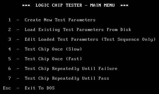
To start the software type "CHIPTEST". If you are using COM2 type "CHIPTEST /2". After a few moments the main menu should appear.
Option 1 allows the creation of new device files, and option 3 allows the editing of the currently loaded file. I will describe these in detail later. For now choose option 2 (press "2"), to load an existing device file. The available files will be listed on the screen (in alphabetical order if you have DOS 5 or later); if there is more than one screen full you will be prompted to press any key to see the next part. Note that the files have only the device base number. For example, 7432 is also suitable for 74LS32, 74HCT32, 5432 etc. from any manufacturer. Similarly 4024 is also suitable for 14024, 74HCT4024 etc.
You will now be prompted to type in the name of a device. Type "7400" if you have one of these devices (or enter the name of another basic logic device that you have available). The file will load and the main menu will reappear. The description below assumes a 7400.
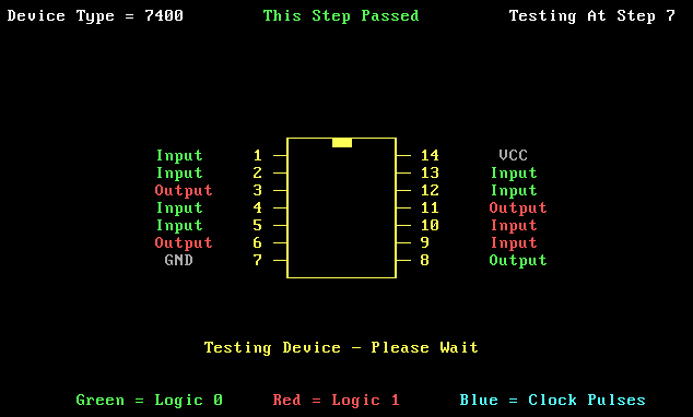
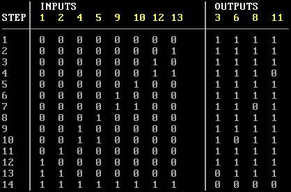
Choose option 4 ("Test Device Once (Slow)"). A picture of a 14-pin device will appear, with instructions about how to fit it into the socket. Here you will be told to place it at the bottom of the socket, and set the power switch to 14. Do as requested then press any key.
The device will be tested one step at a time, and the logic state of each pin is shown using red for high and green for low. The test step number and result of this step (Pass or Fail) is shown at the top of the screen. At the end of the test the overall result is shown - accompanied by a beep if it failed. Hopefully yours passed!
Press any key to get back to the main menu. Choose 5 ("Test Device Once (Fast)") and the device will be tested again somewhat quicker, and without the individual step results. Generally you would use option 4 for debugging test routines and option 5 for actual testing. Option 6 ("Test Device Continually Until Fail") and Option 7 ("Test Device Continually Until Pass") are self explanatory - the number of complete tests completed is shown at the top of the screen.
If you want to see how the unit handles a faulty device, link pins 1 and 2 with a screwdriver and test it again. This fault will be detected because the inputs will not go to the levels they are set to. The testing routine checks the logic levels on all input and clock pins to make sure they are at the level they were set to.
Creating a new device file
We will now go on to create a new device file. We will stick with our 7400 for now, since we know it works! If you don't know this device, dig out a data book or the Maplin catalogue so you can follow what we're doing. Choose option 1 from the main menu and you will be prompted for a device name. Since you already have a good 7400 file which you probably don't want to overwrite, type "TEST" or something similar. You will now be prompted to enter the number of pins, type "14".
A picture of a 14-pin device will now appear, with a question mark by pin 1. You will be prompted to enter a pin type for pin 1, from the seven options at the bottom of the screen. "Input" and "Output" are obvious, "+ve Clock" is a clock pin that is normally low but needs high clock pulses and "-ve Clock" is the opposite of this. "VCC" is the positive supply, "GND" is the negative supply and "Unused" is - well - unused!
Press "1" to make pin 1 an input (no need to press <Enter>). The word "Input" will appear by pin 1 and the question mark will move to pin 2. Since this is also an input press "1" again. Pin 3 is an output so press "2". To finish the pin details enter "1", "1", "2", "6", "2", "1", "1", "2", "1", "1", "5". If you've got all this right, press "Y" to continue, otherwise press "N" to have another go.
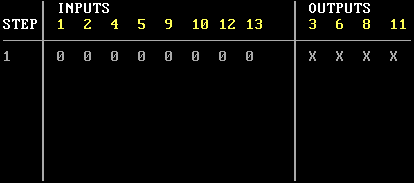
You will now see a screen with pin numbers at the top, and some column dividing lines. Don't worry, it's not as bad as it looks! If there were any clock pins these would be on the left, the inputs come next, followed by the outputs. Dividing lines appear between each group. On the extreme left is the step number.
On this screen you enter the individual steps of the device test. In the input column you enter the logic levels required on the inputs, and in the output column you enter the logic levels expected on the outputs. The inputs may be either 1 or 0, and the outputs may be 1, 0 or X (X = don't care). If there were any clock pins you would enter the number of clock pulses required - the limits here are 9999 if there is one clock input, or 99 if there is more than one.
On line 1, all inputs are low so the outputs are all high. On lines 2 and 3, only one input of one gate is high so in both cases all outputs should still be high. On line 4, both inputs of one gate are high, so that output should go low. The remaining lines repeat these input combinations on the other three gates, and the final line sets all inputs high so all outputs should be low. If you check the device pinouts and truth table this should become clear. The output of a NAND gate will be high unless all inputs are high.
Bear these points in mind when entering test values. The maximum number of test steps is 200. As you go over 22, the screen will scroll up to show the current data line. The arrow keys control the cursor position, and <Enter> will move the cursor to the beginning of the next line. The logic values can be changed by typing the new value, and the cursor will move to the next position. Alternatively tap the space-bar to step through the possible values. The clock pulse numbers can be changed by using <Backspace> to delete the old value then typing the new value. To delete the last line of the test routine, move the cursor onto it and press <Delete>.
When testing the device, the inputs will not all change at exactly the same time. This is not generally a problem, since they will all be at the specified levels by the time the outputs are read back. If it is necessary to change the inputs in a particular sequence this should be done as separate steps.
Clock pulses are applied in pin number order (if there are values in more than one position), and are always applied BEFORE the logic values in that step are set. If it is necessary to set certain logic values on other inputs before applying clock pulses, this should be done as separate steps.
Tri-state output pins in the disabled state will always read high, due to the pullup resistors in the Chiptester. If a device has bidirectional pins it will be necessary to create different test files to accommodate the different directions. See the "74245-A" and "74245-B" files for an example of how to do this.
Type in the values shown, and press <Escape> when finished. You will be asked if you wish to save the data. If you choose "Y" the data will be saves in a file called "TEST.CHP" (all Chiptester data files have the extension ".CHP"). If you chose "N" the data will not be written to disk, but will still exist in memory and can be used to test devices or edited and saved later.
Now try testing the device, to see if your test routine works. If you typed it in correctly it should be OK, but don't worry if not.
Option 3 from the main menu allows the test routine to be edited. This is useful if (or should I say "when") test routines do not work as expected. The pin details cannot be edited since these are not likely to change!
To quit from the software, press <Escape> at the main menu, then answer "Y" to the "Are you Sure" question. Make sure you have saved any changes you want to keep, otherwise your work will be lost.
Over 40 device files are supplied with the software. Some of these have been tested, but there will inevitably be a couple of errors in the others.
Parts
Resistors (all 5% 0.25W)
R1 4M7
R2 2K2
R3 1K0
R4,51 47K
R5-27 (23 off) 4K7
R28-50 (23 off) 220R
R52 330R
RN1 4K7 * 8 SIL Resnet
Capacitors
C1-5 22uF 16V
C6,7 22pF
C8 2n2F
C9 10uF
C10-14 100nF
C15 47uF 16V
Semiconductors
IC1 MAX232
IC2 4060 or 74HCT4060
IC3 CDP6402 (Maplin QQ04E)
IC4 74HCT14
IC5-10 74LS75 or 74HCT75
IC11-14 74LS05 or 7406
IC15 74LS238 or 74HCT238
IC16 74LS138 or 74HCT138
IC17-19 74LS244 or 74HCT244
D1 1N4148
D2 LED
Miscellaneous
XT1 2.4576MHz Crystal
SK1 9 or 25 Way D Connector
SK2 24 Way Universal ZIF Socket
SK3 DC Input Socket
SW1 6 Position Rotary with Knob
FU1 20mm T500mA with PCB holder
PCB, Software, Case, 5V regulated power supply (eg the EPROM PSU on this website)