Imagine being
faced with a dozen or more cable ends, all the same colour and bearing
no identification. The other ends emerge in another part of the
building, and you have no way of knowing which is which.
You could use a continuity tester and a long length of wire to extend
one of the probe leads. But if you had fifty wires, and a five minute
walk from one end to the other, it would take you a good working day just
to trace them all through!
The Multi-core Cable Tracing System presented here is designed to make
this sort job less of a nightmare! The Sender unit is connected
to up to 64 wires at one end, and then the Readout unit is used to indicate
which is which from the other end. The Readout is simply connected
to any two wires at the other end, and the display indicates which wire
number the positive lead is connected to. Unlike some commercial
systems, this system does not require a separate known common connection
between the two units.
The two units are both battery powered, allowing them to be used in situations
where mains power is not readily available. A red LED on each unit
indicated that the battery is OK. If the LED does not light or is
very faint, the battery should be replaced.
PP3 batteries were used in the prototype, but for more regular use larger
capacity 9V batteries would be a better choice, for example six AA cells
in a suitable holder. Low cost 9V plug-in mains adaptors could also
be used. The 2 digit seven segment LED display on the readout unit
is blanked whenever it is not connected to a cable, to conserve battery
life.
This system must never be used on live cables. Ensure both ends
of the cables to be traced are disconnected before using this system.
If in any doubt, check with a test meter. Connection to live cables
will cause damage to this system, and could endanger the operator.
Circuit Design Decisions
With any cable tracing system, a different signal must be sent down
each wire. The signal is then identified at the other end.
Several systems were considered before deciding on the simple solution
used here.
An analogue system using differing voltage levels were ruled out, primarily
because it would not work with my plan of having no specific ground wire
between the two halves of the system. Noise pickup and voltage drops
in long cables could also affect the results.
I then considered a digital coding system, where a different serial code
is sent down each wire. Although this would work well, it would
result in a rather complex design. A system using differing frequencies
was also considered, but again ruled out for reasons of complexity.
Design Considerations
I finally settled on a system that sends different length pulses along
each wire. The receiver simply has to measure the pulse duration
to determine which wire it is connected to. This has the advantage
of being relatively straightforward and cheap.
The only potential problem is that the capacitance of long cables might
affect the pulse shape. By using logic devices with symmetrical
outputs to drive the cable (74HC series logic), any pulse shaping distortion
should occur equally on the rising and falling edges. This works
well in practice, providing the receiving device has a Schmitt trigger
input. The clock frequency is fairly low, so any distortion in the
pulse shape would have to fairly severe before the reading accuracy would
be affected.
If use with long cable lengths is likely, I would suggest using 74AC logic
devices for the output drive. 74AC devices have an output drive
of +/- 16mA compared to +/- 4mA for 74HC, so they should be less affected
by capacitive loads. However they are not so readily available,
and are typically two or three times the price of 74HC devices.
74LS devices are not really suitable due to having non-symmetrical outputs
(they can sink 8mA but only source 400uA).
Only one wire is driven at a time. This is necessary to fulfill
the requirement of not having a common ground wire. All output lines
are normally high, and a low pulse appears on each wire in turn.
The total time taken to cycle round all outputs is approximately half
a second
The readout unit has two probes, which for clarity I will refer to as
the "Reading" probe and the "Non-Reading" probe. The display on
the readout indicates the number of the wire that the "Reading" probe
is connected to. The "Non-Reading" probe may be connected to any
other wire. Please remember that the power rails in the Sender and
Readout units are not linked together, so some sort of reference is needed.
The "Non-Reading" probe is internally connected to the readout positive
rail. The level on the "Reading" probe therefore goes low for a
period, depending on which wire it is connected to. Then the wire
that the "Non-Reading" probe is connected to goes low, this effectively
results in the "Reading" probe going 5V higher than a logic high level.
This does not reach the logic devices due to a resistor-diode circuit,
and is ignored.
Hopefully this is clear - it is not the easiest arrangement to describe!
Circuit Operation - Sender Unit
We will start with the Sender unit. The complete circuit is
shown in figure #.
IC1a and IC1b (4093) form an oscillator running at about 5KHz. This
drives a 4024 counter (IC2). The outputs of IC2 and another counter
(IC3) are compared by a logic comparator (IC4), the output of which goes
low when the two inputs are equal. This resets IC2 and increments
IC3.
Assume the decimal value of the outputs of IC3 is at ten. Also assume
IC2 has just been reset, so the value of it's outputs is zero. These
two output values are not equal, so the output on pin 19 of IC4 is high.
Once IC2 has received ten clock pulses from the oscillator, it's output
will be equal to that of IC3, and the output of IC4 will go low.
This will increment IC3 so it's output value is eleven, and also reset
IC2 so it's output value is again zero. As soon as this occurs the
counter outputs are no longer equal so the output of IC4 will go high
again. The sequence now repeats, but this time eleven clock pulses
are needed before the two counter outputs are equal.
The outputs of IC3 are decoded into 64 individual outputs by IC5 through
IC13. The 74HC138 is a three to eight line decoder, with active-low
outputs. IC5 decodes into banks of eight, which are then individually
decoded by IC6 to IC13
Therefore each of these decoded lines will go low in turn, for a period
determined by the number of clock cycles needed for the two counter outputs
to become equal. Referring to the previous examples, the "10" output
(SK11) will be low for ten clock cycles, and the "11" (SK12) output will
be low for eleven clock cycles. The output number is the SK terminal
number less one.
Output "0" from SK1 will be low for a very short duration, set by the
values of C7 and R6. This may not work properly in practice, so
it may be better to just use outputs "1" to "63". The delay components
were found to be necessary to ensure IC2 resets correctly and IC3 increments
correctly.
If less than the full 64 outputs are required, you can omit some of the
higher numbered 74HC138 devices. In this case, connect a wire from
the pin 4 position of the first omitted device to SK66. This will
cause the counter system to be reset when the missing device is reached,
speeding up the process by not generating unwanted outputs.
I originally planned to run the circuit from a 6V battery with a diode
to drop 0.7V. However the frequency of the oscillator was found
to vary with supply voltage, so the output pulse durations would vary
as the battery ran down.
Instead I have used a 78L05 regulator, run from a 9V battery. The
LED (D1) across the regulator lights when the voltage across it exceeds
about 2.5V, indicating that the battery is OK. The LED series resistor
(R4) has a high value to ensure insufficient current flows through it
to disturb the action of the regulator. If you are using a higher
voltage battery or a mains power supply unit, you may need to increase
R4 further, or omit D1 and R4 completely.
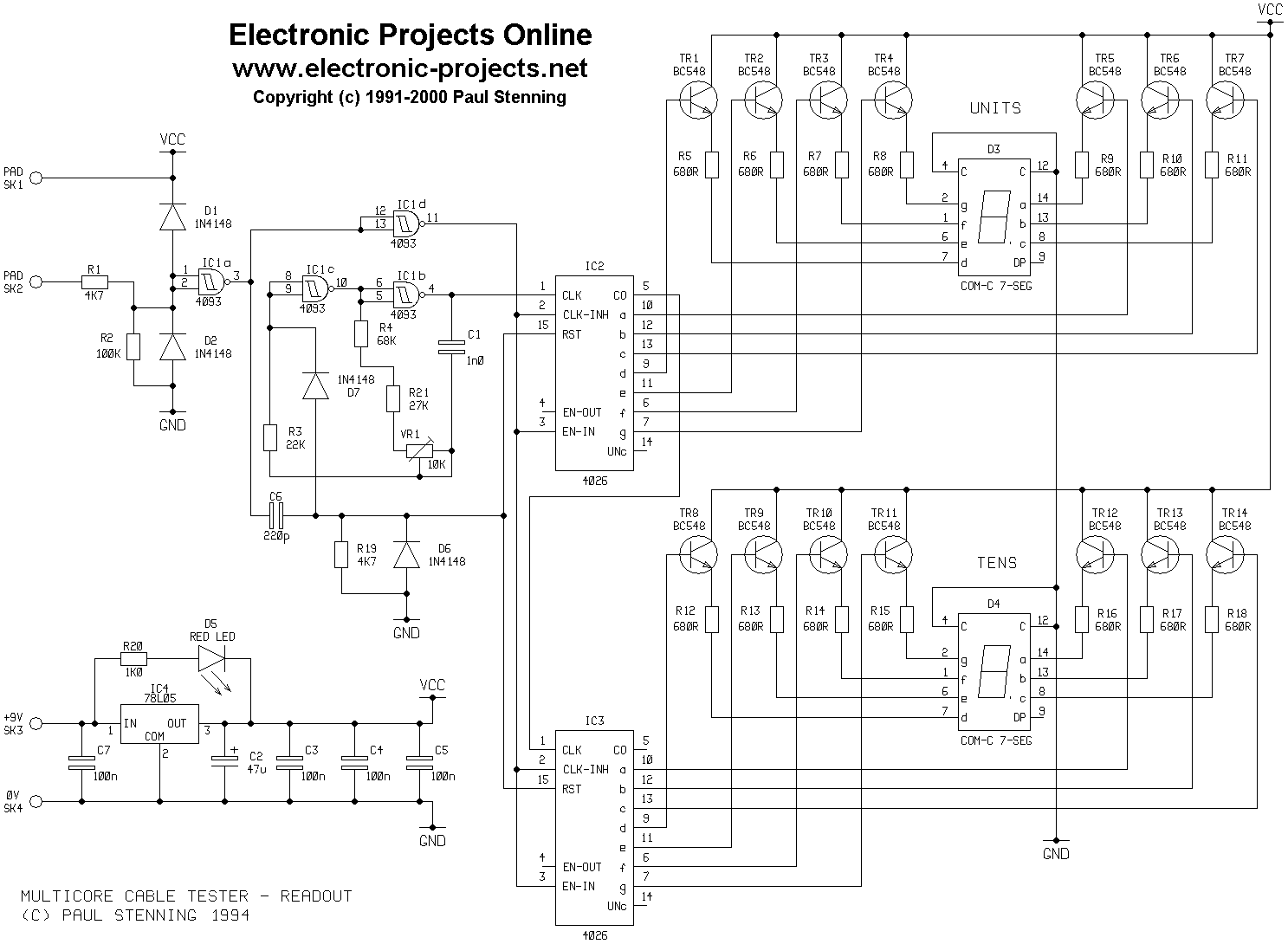
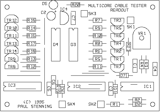
Circuit Operation - Readout Unit
Note that the component reference numbers start at 1 on both the Sender
and Readout. Try not to get confused!
IC1b and IC1c form an oscillator, the same as the one in the sender unit.
One resistor value is variable over a range of +/- 10%, so that the unit
may be calibrated. The output is connected to the Clock input of
IC2
The frequency of this type of oscillator varies with different makes of
4093 IC. To avoid any problems use the same make of 4093 IC in the
Sender and Readout units. This can usually be assured by purchasing
them from the same place at the same time.
IC2 and IC3 are decimal counters with decoded 7 segment outputs.
These outputs are connected to the displays via emitter follower circuits.
The carry output (CO) of IC2 is connected to the clock input of IC3, so
IC3 is incremented when IC2 steps from nine to zero. IC3 thus drives
the tens display while IC2 counts the units.
The test probes are connected to SK1 ("Non-Reading") and SK2 ("Reading").
The "Reading" input is protected by R1, D1 and D2, as described earlier.
R2 holds the input low when it is not connected, blanking the display
to conserve battery power. IC1a inverts the signal. When the
unit is connected to the Sender, the output of IC1a is normally low, and
goes high on the Sender output pulse.
When the input is high (IC1a output low), the clock inhibit inputs (pin
2) of IC2 and IC3 are held high (via IC1d), so that the counters do not
respond to the clock input. The display enable inputs (pin 3) are
also held high, so the displays are illuminated.
When the input goes low, the reset inputs (pin 15) of IC2 and IC3 are
pulsed high momentarily high, reseting the counters. This brief
reset pulse is also coupled to the oscillator via D7, to bring the oscillator
into line with the Sender unit. The clock inhibit input goes low,
allowing the counters to count the clock pulses and the display enable
inputs also go low, blanking the displays. This blanking period
is brief, and hardly visible in practice.
When the input goes high again, the displays show the number the counters
reached. This number depends on the length of time the input was
low, and is therefore the wire number.
The power supply arrangement is identical to that in the Sender unit.
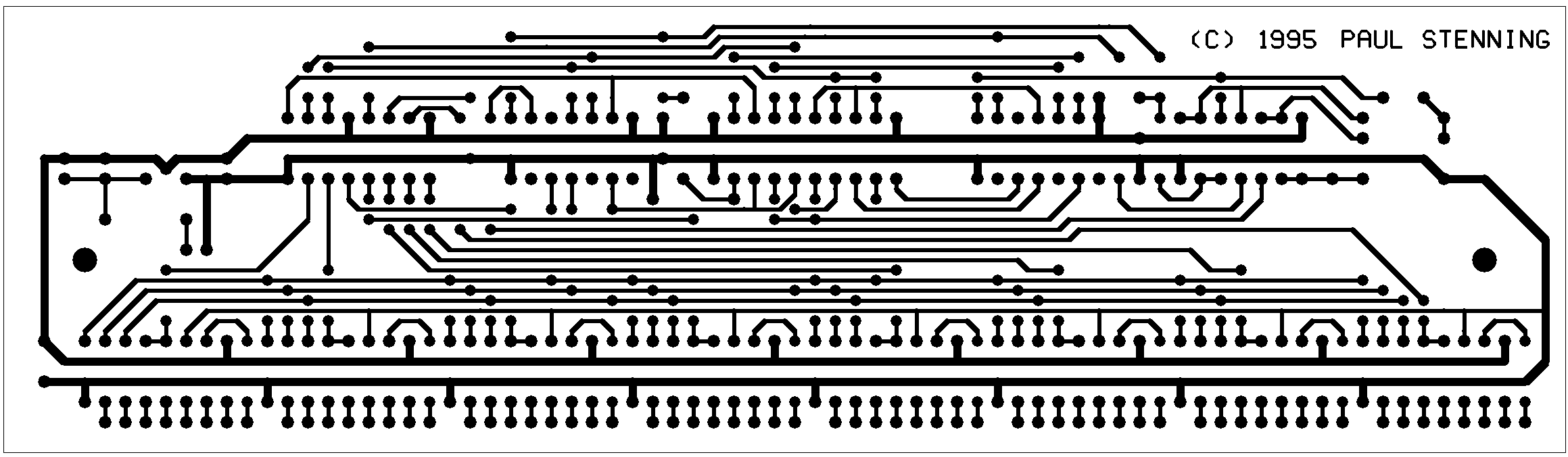
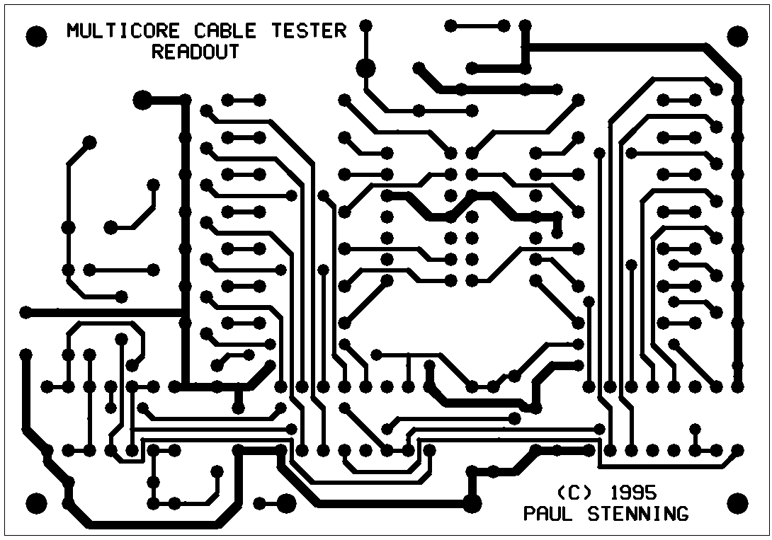
PCB Construction
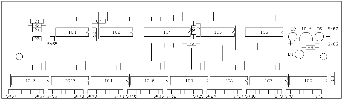
Because both PCB's use the same component references, the parts list
has been divided into two distinct sections. To save confusion,
it may be easier to completely build one PCB at a time.
The PCB construction is very straightforward, and requires little comment
from me. Note that some wire links pass under components, so these
should be fitted first. Use terminal pins or single-in-line header
strip for the off-board components - particularly on the Sender PCB -
these will make wiring up much easier. Drill a hole in the Readout
PCB below VR1 to allow it to be adjusted once it is fitted into the case.
Do not fit the LED's yet. In the Sender unit the LED is mounted
on the case, so terminal pins should be fitted in the PCB. In the
Readout the LED has to fit through a hole in the case so it would be better
to solder it once everything has been lined up.
On the prototype, the IC's and LED displays were soldered directly into
the PCB. You may find it useful to use sockets for the displays
to space them away from the PCB.
You may also wish to fit the IC's in sockets, particularly IC6 through
IC13 on the Sender unit, since these are most likely to be damaged if
the unit is inadvertently connected to low voltage live wires. The
same applies to IC1 on the Readout unit. If the units are accidentally
connected to live mains voltage wiring, they will almost certainly be
damaged beyond repair.
Sender Unit Case
The sender unit fits neatly in a low cost plastic box, type MB6, which
is readily available. Everything is constructed on the lid, simplifying
construction.
The lid overlay is shown in figure #. This diagram could be photocopied
and used as a drilling template. An additional copy can be fixed
to the lid before finally mounting the components.
Low cost 5A terminal block was used for the cable connections on the prototype.
Wires from one side pass through small (1.5mm) holes in the box, to reach
the PCB. Push these wires through from the outside, to avoid lifting
the overlay.
You could use barrier strip connectors (the type with one screw terminal
and a rear solder tag) but this is more expensive.
It is obviously not necessary to use every fixing hole in the terminal
block connectors, four screws per 12 way length are sufficient.
M3 screws and nuts are ideal. The PCB mounts on the two end fixing
screws of the middle row of terminal block. If you fit 12mm spacers
in place of the nuts on these two screws, the PCB can be fixed to them
with two short M3 screws.
The LED is fitted in a normal LED clip, which requires a 6.5mm hole.
A rectangular cutout is needed for the power switch (a small slide switch).
However if you are using figure # as an overlay you could just drill a
large round hole and let the overlay hide it! The slide switches
are not normally supplied with M2 fixing screws, so you will need to order
these separately.
The interwiring is very straightforward. Firstly each terminal on
the outside of the case is connected to the appropriately marked point
on the PCB. Take care to get these correct, although any errors
will show up during testing.
The LED should then be connected to the appropriate points on the PCB.
If you are in any doubt about the LED pinouts, hold it up to the light
so you can see it's innards. The anode lead connects to the smaller
internal piece to one side, and the cathode to the larger piece with a
cupped shape in the top middle. This is easy to remember if you
think of Cup for Cathode and Arm for Anode (same initial letters).
This simple method of lead identification holds true for all conventional
single colour visible LED's and most IR LED's. However it should
not be relied on for some of the more fancy LED's such as the multi-colour,
flashing and low current types.
The LED anode connects to the pin closest to the edge of the PCB.
Finally connect the battery lead and the switch to the PCB. The
battery negative (black) lead goes to SK66, and the battery positive (red)
lead goes to the centre pin of the switch. Connect a piece of wire
between SK67 on the PCB and the uppermost switch terminal.
On the prototype the PP3 battery was retained with a self-adhesive 'C'
shaped cable clip. A double sided sticky pad may be a more readily
available solution. If you are using a larger capacity battery such
as 6 AA cells in a suitable holder, you will need to devise some method
of securing this. Check that your proposed battery holder will fit
the case before ordering it - you may need to use two or more smaller
battery holders wired in series.
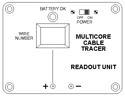
Readout Unit Case
The prototype readout unit was constructed in a type MB2 case.
However this was rather too tight for comfort, and the corners of the
PCB had to be filed down. An MB3 type is slightly bigger and would
be a better choice. If you want to use a higher capacity battery
you may need something larger still.
The front panel overlay of the prototype is shown in figure #. This
may be of limited use if you are not using an MB2 case, but it does give
some idea of the layout.
You will need to make a rectangular hole for the LED displays to show
through. As mentioned previously, by using an overlay you can hide
any irregularities in your cutting. A piece of red filter material
fitted behind the cutout will dramatically improve the contrast if the
display.
The PCB is spaced away from the box lid with 12mm long spacers.
On the prototype a piece of plastic sheet (available from model shops)
was fitted behind the PCB, to prevent the battery causing short circuits.
This adequately retained the battery in the MB2 case, but if you are using
an MB3 case you may need to add some foam to stop it rattling.
Before finally fixing the PCB, the wiring should be completed. The
LED solders directly into the PCB, however you will need to form the leads
to allow it to show through the hole in the case. You may need to
sleeve the leads to prevent them shorting. The LED anode connection
on the PCB is closest to R20.
Battery negative connects to SK4 and battery positive connects to SK3
via the switch. The positive (+) test-lead (the "Reading" lead)
connects to SK2, and the negative (-) to SK1. These leads pass through
the small holes shown in the case and the free ends may be fitted with
crocodile clips or similar. Knot the cables inside the case to save
straining the PCB if they are pulled.
Testing
If you constructed the units carefully and luck is on your side, they
should work first time. All you would then have to do is calibrate
the Readout unit.
Initially it is best to test the units by connecting the directly together.
Once this is working OK, you can try them with a length of multi-core
cable.
Switch the Readout unit on. The 'Battery OK' LED should light, and
the display should be blank. Touch the two test leads together and
the display should light up, and show a number between 00 and 99.
It is most likely to show 00 due to contact bounce as you touch the probes
together. If you can get it to show a number other than 00 (by touching
the probes together abruptly), you can be confident that it is working
OK.
Now switch the Sender unit on. It should not do anything exciting
but the LED should light.
Connect the positive readout probe to terminal 63 on the Sender, and connect
the negative to any other terminal. The display should show a steady
number, although it may alternate between two adjacent numbers.
You should just be able to see the display flicker about twice a second.
Adjust VR1 in the Sender until the display indicates 63. Find the
points where the reading alternates between 62 and 63, and between 63
and 64. Set the preset mid-way between these two points.
If the preset does not have enough range, you may need to adjust the value
of R4 or R21. If the two 1n0 timing capacitors and the two 4093
IC's are from the same batches (bought from the same place at the same
time), you should have no problems.
Now try connecting the positive probe to each of the other terminals in
turn. You should get the appropriate number displayed. You
may get one number as the probe is connected, followed by another which
remains constant. In this case just ignore the first number.
As mentioned previously, the zero output may not work correctly due to
the pulse being so short. If this is the case you would be best
just to ignore it.
If you are building more than one pair of units, please note that they
are calibrated in pairs. Clearly mark the units so that the right
units are always used together.
Longer Cables
If you have a long piece of multi-core cable to hand, try the units
on it. It is not possible to give a maximum permissible cable length
since this depends mainly on the capacitance, which in turn depends on
the cable construction. In the case of individual wires, it depends
on how they are installed, for example whether they are in metal conduit
and how closely they are packed.
If you have problems with long lengths of cable affecting the readings,
there are a couple of things you can try. Firstly you could try
using 74AC138 devices for the output drive, as described earlier.
Secondly you can try decreasing the clock speed. Simply increase
the values of both C1 capacitors. Remember to re-adjust VR1 after
changing any values.
The problem is caused by the edges not rising and falling quickly.
If the total rise and fall time exceeds about half a clock period, there
is a possibility of inaccuracy. By slowing the clock, we effectively
widen the acceptance range.
The drawback with this is that the time taken to get a valid reading will
increase, although even if it takes several seconds it is still much quicker
than messing around with a multimeter. If the capacitors are increased
to 10n, the time to get a valid reading will be no more than five seconds,
which seems reasonable and should allow vast lengths of cable to be identified
with no problems. This is probably the largest practical capacitor
value.
If you will only be testing a limited number of wires, you can reduce
this time delay by removing one or more of the output IC's and connecting
the pin 2 position of the first empty IC space to SK65 (see circuit description
earlier). The time saving obtained can be quite significant since
the higher numbers take more time than the lower numbers.
Parts List - Sender Unit
Resistors (all 5% 0.25W
or better)
R1
22K
R2
100K
R3,R5
4K7
R4,R6
1K0
Capacitors
C1
1n0
C2
10u 25V Radial Elect
C3,C4,C5
100n
C6
2u2 35V Radial Elect
C7
470p
Semiconductors
IC1
4093 Quad NAND Gate
IC2,IC3
4024 7 Stage Binary Counter
IC4
74HC688 8 Bit Logic Comparitor
IC5,IC6,IC7,IC8,IC9,
IC10,IC11,IC12,IC13
74HC138 3 to 8 Line Decoder
IC14
78L05 5V 100mA Voltage Regulator
D1
RED LED
Miscellaneous
Case type MB6, PCB code ???, Terminal block (6 off), SPDT slide switch,
LED clip, PP3 battery, PP3 battery clip, wire.
Parts
List - Readout Unit
Resistors (all 5% 0.25W
or better)
R1,R19
4K7
R2
100K
R3
22K
R4
68K
R5,R6,R7,R8,R9,R10,R11,R12,
R13,R14,R15,R16,R17,R18 680R
R20
1K0
R21
27K
VR1
10K Horizontal preset
Capacitors
C1
1n0
C2
47u 16V Radial Elect
C3,C4,C5,C7
100n
C6
220p
Semiconductors
IC1
4093 Quad NAND Gate
IC2,IC3
4026 Decimal counter (7 seg output)
IC4
78L05 5V 100mA Voltage regulators
TR1,TR2,TR3,TR4,TR5,
TR6,TR7,TR8,TR9,TR10,
TR11,TR12,TR13,TR14
BC548 NPN Transistor
D1,D2,D6,D7
1N4148 Diode
D3,D4
0.3" Com Cathode Red 7 Seg LED Display
D5
RED LED
Miscellaneous
Case type MB2, PCB, Red and black croc-clips, SPDT slide switch, Red LED
filter material, LED clip, PP3 battery, PP3 battery clip, wire